
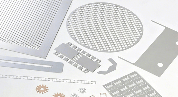
0.01mm Stainless Steel Foil Chemical Etching: Process Advantages, Features & Applications
0.01mm (10 micron) stainless steel foil is an ultra-thin engineering material valued for its high tensile strength, excellent corrosion resistance and stable electrical conductivity, making it indispensable in high-end sectors including microelectronics, medical devices and precision instrumentation. However, its extremely thin gauge poses major challenges for traditional fabrication methods: stamping often causes foil tearing and edge curling, laser cutting leaves a heat-affected zone and thermal warping, and mechanical drilling suffers from severe burrs and high scrap rates. None of these conventional processes can reliably deliver high-precision micro components on such thin substrates. Chemical etching, a non-contact cold manufacturing technology, overcomes these bottlenecks by combining high-resolution photolithographic pattern transfer with controlled liquid-phase chemical dissolution. It produces precision micro-structures on 0.01mm stainless steel foil with micron-level accuracy, zero residual stress and excellent batch consistency, and has become the preferred processing solution for ultra-thin precision stainless steel components.
I. Core Technical Features of 0.01mm Stainless Steel Foil Chemical Etching
The room-temperature liquid-phase reaction mechanism gives chemical etching inherent technical advantages unmatched by traditional fabrication methods for ultra-thin foils. These features directly determine the dimensional accuracy, functional performance and total cost of ownership of finished parts.
1. Room-Temperature Cold Forming with Zero Stress & Thermal Damage
Chemical etching operates entirely at ambient temperature in a liquid environment, applying no mechanical punching force and introducing no high-temperature thermal input to the 0.01mm stainless steel foil. Material is removed through uniform molecular-level dissolution rather than mechanical shearing or thermal ablation, eliminating common defects of traditional processes such as foil tearing, warping, work hardening and heat-affected zones. The process fully retains the base material’s native mechanical strength, elasticity, corrosion resistance and electrical conductivity, and avoids stress concentration and fatigue cracking risks. This is particularly critical for high-reliability applications where even minor deformation can lead to functional failure.
2. Micron-Level Accuracy with Excellent Full-Sheet Uniformity
For 0.01mm ultra-thin stainless steel foil, mature chemical etching processes deliver a stable dimensional tolerance of ±0.005mm, with a minimum machinable line width of 0.015mm and minimum through-hole diameter of approximately 1.1 times the material thickness. Since all features form simultaneously through uniform chemical reaction across the entire sheet, there is no cumulative positioning error, and dimensional consistency across the full workpiece exceeds 99.5%. Unlike laser cutting which suffers from sequential positioning deviation, or stamping which faces die wear and springback errors, chemical etching ensures every micro feature on the foil maintains uniform dimensions, which is essential for high-density components such as micro filter arrays and fine-pitch contacts.
3. Burr-Free Smooth Edges with No Secondary Finishing Required
The molecular-level dissolution mechanism produces smooth, rounded edges completely free of burrs, flash, slag nodules and sharp protrusions. For most industrial applications, etched 0.01mm stainless steel parts can proceed directly to assembly without secondary deburring, grinding or polishing. Compared with punched and laser-cut foils that often leave sharp burrs and loose metal particles, chemically etched components eliminate risks such as filter clogging, circuit shorting and tissue scratching during service. This burr-free property also makes the process highly suitable for high-cleanliness scenarios including medical devices and semiconductor manufacturing.
4. Design Freedom with No Complexity Premium
There is no geometric complexity penalty in chemical etching. It supports all types of aperture geometries including round holes, square openings, elongated slits and custom irregular shapes, as well as flexible layout patterns such as staggered, orthogonal and variable-density arrangements. Production starts immediately after importing digital CAD files, with no dedicated hard tooling required. Design revisions only need an updated photomask file, with no additional mold modification costs or long debugging lead times. This gives engineers complete freedom to optimize part structures for functional performance, without being constrained by manufacturing process limits.
5. Stable Batch Consistency Without Tool Wear Drift
Chemical etching production runs on fully automated closed-loop systems that maintain precise, constant control over etchant concentration, temperature, spray pressure and conveyor speed. Since there is no physical tool to wear out, dimensional accuracy and edge quality remain completely consistent from the first part to the millionth part, with no gradual quality degradation over extended production runs. This long-term batch-to-batch repeatability meets strict quality traceability requirements for medical, automotive and aerospace customers, reduces incoming inspection workload and improves overall production efficiency.
6. Precision Half-Etching for Integrated 3D Micro-Features
Beyond full through-etching for complete part separation, chemical etching supports highly accurate half-etching for partial-depth surface features on 0.01mm stainless steel foil. By tightly controlling processing duration, partial-depth recesses can be created with depth tolerance controlled within ±0.003mm. This enables integrated formation of positioning grooves, sealing recesses and step structures in a single process step, eliminating secondary machining operations and improving assembly alignment accuracy. Half-etching is a unique advantage of chemical etching that cannot be easily achieved by stamping or laser processes for ultra-thin foils.
7. Full Retention of Native Material Properties
Unlike mechanical and thermal processes that alter material microstructure and degrade performance, chemical etching preserves 100% of the stainless steel foil’s native corrosion resistance, fatigue strength and electrical conductivity. There is no intergranular corrosion risk from heat exposure, and no reduction in elastic performance from work hardening. This property ensures long-term stable performance of parts in harsh environments such as high humidity, salt spray and corrosive media, meeting the strict reliability requirements of high-end industrial applications.
II. Core Functions & Industrial Value
Beyond basic micro-structure forming, chemically etched 0.01mm stainless steel components deliver six core functional values, solving long-standing pain points in precision manufacturing and creating tangible economic benefits for downstream industries.
1. Precision Micro-Filtration & Stable Fluid Regulation
The most widely applied function is precision micro-filtration and flow control. Uniformly sized micron apertures deliver accurate particle interception and stable flow resistance across the entire filter surface. Smooth, burr-free hole walls prevent particle clogging and maintain consistent flow rates over long service lives, avoiding the gradual resistance increase common with woven screens and punched filters. This function is indispensable in medical infusion systems, microfluidic devices, hydraulic precision filtration and chemical reagent processing.
2. Micro Elastic Contact & Reliable Electrical Interconnection
Etched micro spring contacts and connector springs provide reliable electrical connection and consistent elastic preload. The stress-free forming process preserves the full elastic properties of the stainless steel foil, delivering stable contact force and extended fatigue life. They maintain consistent contact resistance through millions of insertion cycles, avoiding signal interruption caused by poor contact, and are widely used in miniature connectors, consumer electronics circuits and semiconductor packaging components.
3. Lightweight Integrated Micro-Structure Forming
Chemical etching enables integration of multiple functional features — including filter holes, elastic beams, mounting holes and positioning notches — onto a single 0.01mm stainless steel foil in one processing step. This eliminates the need to assemble multiple separate micro components, reduces overall product volume and weight, improves structural reliability and lowers total system cost. For miniaturized devices such as medical implants and wearable electronics, integrated design can reduce component size by more than 30%.
4. Damage-Free Processing for High-Reliability Components
For fatigue-sensitive and heat-sensitive components used in aerospace and medical applications, chemical etching delivers nearly damage-free processing with zero mechanical stress and zero thermal impact. It does not alter the material’s crystal structure or degrade native mechanical and corrosion-resistant properties, directly improving long-term product reliability and service life. This is particularly critical for safety-critical parts that operate in extreme environments.
5. Rapid Prototyping & Agile R&D Iteration
Low-cost digital photomask tooling enables chemical etching to deliver prototype samples within 24–48 hours, supporting rapid iterative verification of new product designs. There is no expensive hard tooling investment, which greatly reduces R&D trial-and-error costs and shortens overall product development cycles. This helps enterprises bring new products to market faster and maintain competitive advantage in fast-evolving high-tech sectors.
6. Optimized Total Manufacturing Cost
Although the unit processing cost is slightly higher than high-volume stamping, chemical etching eliminates expensive mold costs, reduces secondary deburring and finishing operations, and achieves higher production yield. For small and medium batch orders, customized products and ultra-thin foil components, the total manufacturing cost of precision chemical etching is significantly lower than traditional processes. It also reduces quality management overhead and delivery lead times, helping enterprises optimize overall supply chain efficiency.
III. Key Industrial Application Fields
Thanks to its unique combination of precision, flexibility and material compatibility, chemical etching of 0.01mm stainless steel foil serves a growing range of high-tech and industrial sectors.
1. Electronics & Semiconductor Advanced Packaging
This is the largest and fastest growing application field. Common components include ultra-fine pitch lead frames, miniaturized EMI shielding cans, vapor chamber wick structures and micro connector spring contacts. The process’s micron-level accuracy, burr-free quality and stress-free structure perfectly support the ongoing trend toward smaller, denser and more reliable electronic and semiconductor packaging.
2. Medical Devices & Life Sciences
Medical-grade etched components include infusion filter meshes, implantable electrodes, biosensor chips and surgical instrument micro accessories. Burr-free surfaces, biocompatibility and resistance to autoclave sterilization comply with strict medical safety standards. The technology enables advanced medical applications from minimally invasive surgical instruments to in-vitro diagnostic devices.
3. Precision Instrumentation & Optical Equipment
Chemical etching produces optical slits, diaphragms, encoder gratings and precision shims for spectrometers, laser systems, industrial cameras and precision measuring instruments. Micron-level edge accuracy and burr-free sharp edges ensure excellent optical performance, avoiding stray light and diffraction noise, and providing reliable optical path control for various optoelectronic systems.
4. Aerospace & High-End Equipment
Aerospace manufacturers use 0.01mm etched parts including ultra-thin precision shims, micro hydraulic filter screens and sensor components for aircraft and satellite systems. Full material property retention, stress-free stability and high fatigue reliability meet the extreme reliability demands of aerospace applications, where parts must withstand wide temperature ranges, intense vibration and corrosive environments over decades of service.
5. New Energy & Energy Storage Systems
In new energy and energy storage sectors, 0.01mm stainless steel etched meshes serve as micro current collectors, electrode substrates and flow field structures for micro fuel cells and supercapacitors. Uniform pore distribution ensures uniform current density and reaction interface area, improving energy density and cycle life of energy storage devices. The ultra-thin foil substrate also supports lightweight design of battery systems.
6. Industrial Automation & Motion Control
Etched micro encoder discs, precision shims, flow orifice plates and flat springs are foundational components in micro servo motors, precision positioning stages and automated production lines. They deliver stable, high-accuracy position feedback and reliable fluid control required for modern smart manufacturing, ensuring consistent production quality and equipment uptime.
7. Consumer Electronics & Wearable Devices
Smartphones, wireless earbuds, smart watches and wearable devices incorporate a wide range of 0.01mm etched parts, including ultra-fine speaker dust meshes, camera VCM springs and micro EMI shielding structures. Ultra-thin forming capability, high pattern density and mass production consistency perfectly match the consumer electronics industry’s requirements for slim design, miniaturization and stable large-scale supply.
Conclusion
In summary, chemical etching breaks through the processing bottleneck of traditional technologies for 0.01mm ultra-thin stainless steel foil, delivering a high-quality, flexible and efficient manufacturing solution with core advantages of micron-level accuracy, zero stress, burr-free edges and tooling-free customization. It strongly supports performance upgrades across electronics, medical, semiconductor and other industries, and has become an indispensable precision manufacturing technology for ultra-thin metal micro components.
As global products continue to advance toward miniaturization, higher integration and better reliability, market demand for 10-micron grade ultra-precision stainless steel components will continue to grow. Looking ahead, chemical etching technology will continue to evolve toward higher resolution, tighter process control and wider material compatibility, further expanding its application scope and providing stronger technical support for product innovation and industrial upgrading in more high-end manufacturing sectors.