
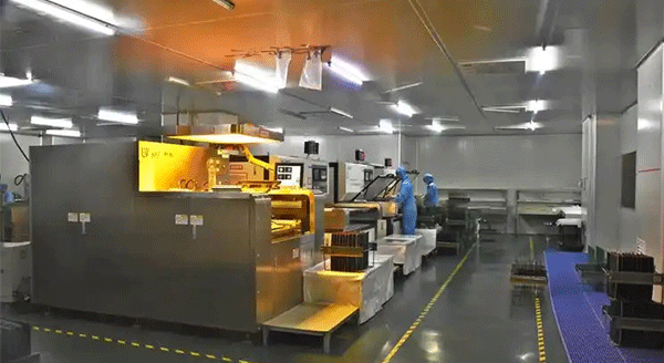
How to Do Photo Etching: Full Step-by-Step Process Guide, Features & Applications
Photo etching, also referred to as photochemical machining, is a non-contact cold subtractive manufacturing technology that produces custom precision metal components via photolithographic pattern transfer and controlled chemical dissolution. For engineering teams, product designers and manufacturing practitioners looking to evaluate or adopt this technology, clarifying how to do photo etching with a standardized, repeatable workflow is the foundational step for process validation and production implementation. Unlike traditional stamping, laser cutting and CNC milling that rely on mechanical force or thermal energy to remove material, photo etching shapes workpieces at the molecular level under ambient temperature, delivering unique advantages in dimensional accuracy, detail resolution and design freedom. This article breaks down the complete step-by-step photo etching workflow, and systematically introduces its core process characteristics, functional values and main industrial application scenarios.
I. Step-by-Step Photo Etching Workflow
The standard industrial photo etching process follows seven core sequential steps, with strict parameter control at each stage to ensure final part accuracy and quality.
1. Material Preparation & Surface Cleaning
First, select the appropriate metal grade and sheet thickness according to part performance requirements, and cut the raw material to standard production dimensions. Then perform thorough surface cleaning to remove oil stains, oxide layers and dust particles on the metal surface, ensuring sufficient adhesion between the photoresist and the substrate. Poor cleaning will cause photoresist peeling and pattern defects during subsequent etching, making this a critical pre-process quality control node.
2. Photoresist Coating & Curing
Coat a uniform layer of UV-sensitive photoresist on both sides of the cleaned metal sheet through precision roller coating, then send it to a constant-temperature drying oven to cure the photoresist layer. Coating thickness is precisely adjusted according to material thickness and target etching depth, ensuring stable corrosion resistance throughout the etching stage.
3. Photomask Alignment & UV Exposure
Fit the high-precision photomask film plotted directly from CAD files tightly onto the photoresist-coated sheet, and perform double-sided alignment exposure under a precision UV exposure machine. The photoresist in the irradiated area undergoes a cross-linking curing reaction, forming a corrosion-resistant protective layer that exactly matches the design pattern. The alignment accuracy of this step directly determines the final dimensional precision of finished parts.
4. Developing & Pre-Etching Inspection
Rinse the exposed sheet with dilute alkaline developer to dissolve and remove the unexposed photoresist, leaving the cured protective pattern on the metal surface. After developing, conduct full visual and dimensional inspection to confirm pattern integrity, position accuracy and no defects. Only qualified workpieces can proceed to the etching process.
5. Controlled Chemical Etching
Send the developed sheet into a horizontal conveyor etching machine, and spray the formulated etchant solution evenly on the workpiece surface under constant temperature and pressure. The unprotected metal area is uniformly dissolved by the etchant, and etching depth is precisely controlled by adjusting conveyor speed, solution concentration and temperature. Both full through-etching for part separation and half-etching for partial depth structures can be achieved in this single step.
6. Photoresist Stripping & Clean Rinse
After etching reaches the target depth, immerse the workpiece in a dedicated stripping solution to completely remove the remaining cured photoresist, then rinse repeatedly with deionized water to remove all residual chemical substances. This step ensures no foreign matter remains on the finished part surface, meeting cleanliness requirements for industrial, electronic and medical applications.
7. Final Inspection & Optional Post-Treatment
Conduct final dimensional, appearance and functional inspection on finished parts, and carry out optional post-treatments such as deburring, polishing, anodizing or passivation according to project requirements. Qualified finished parts are packaged and delivered after passing full quality inspection.
II. Core Characteristics of the Photo Etching Process
The room-temperature chemical forming mechanism gives photo etching a set of inherent technical advantages that traditional processing methods cannot match, which are also the core reasons for its wide adoption in high-precision manufacturing.
1. Burr-Free Stress-Free Cold Forming
As a pure room-temperature cold process, photo etching applies no mechanical extrusion or high-temperature thermal impact to the substrate, introducing zero residual stress, lattice deformation or heat-affected zone. Edges formed by molecular dissolution are smooth and evenly rounded, completely free of burrs and sharp protrusions, and 100% retain the native mechanical, electrical and corrosion resistance properties of the base material.
2. Micron-Level Accuracy & High Pattern Fidelity
Standard photo etching achieves stable dimensional tolerances of ±0.005mm to ±0.01mm, with a minimum machinable line width of 0.02mm. All features across the entire production sheet form simultaneously through uniform chemical reaction, with no cumulative positioning error, and batch dimensional consistency exceeds 99.5%, far exceeding the level of traditional mechanical processing.
3. Zero Complexity Premium & Unlimited Design Freedom
There is no additional cost for geometric complexity in photo etching. Complex curves, dense micro-hole arrays and irregular custom contours all carry the same unit cost as simple basic shapes, and are formed in a single process step. Design modifications only require updating the digital file and remaking the photomask, with low cost and short lead time, making it highly suitable for multi-variety, small-batch customized production.
4. Precise Half-Etching & Integrated 3D Features
In addition to full through-etching for part separation, photo etching supports highly accurate half-etching with depth tolerance controlled within ±0.005mm. It can form three-dimensional structures such as positioning grooves, sealing grooves and decorative textures on the sheet surface, realizing integrated functional design and reducing secondary processing procedures.
5. Wide Material Compatibility & Stable Batch Consistency
Photo etching is compatible with almost all common engineering metals, including stainless steel, copper alloy, aluminum alloy, titanium alloy and nickel-based alloy. The automated closed-loop production system maintains stable process parameters, and quality remains completely consistent from the first part to the millionth part, with no quality drift caused by tool wear.
6. Low-Cost Rapid Tooling & Agile Prototyping
Photo etching uses low-cost digital photomask films as tooling instead of expensive hardened steel dies. The tooling cost is less than 1/50 of stamping dies, and prototype samples can be delivered within 24–48 hours after drawing confirmation, greatly shortening product R&D cycles and reducing trial-and-error costs.
III. Core Functions & Industrial Values
As a precision manufacturing technology, photo etching delivers six core functional values for downstream industries, solving common pain points in traditional processing and creating tangible economic benefits.
1. Precision Filtration & Stable Flow Control
Uniformly sized micron apertures achieve accurate particle interception and stable flow resistance. Smooth, burr-free hole walls avoid clogging, ensuring long-term stable operation of fluid systems, which is widely used in hydraulic equipment, beverage processing and water treatment fields.
2. Reliable Elastic Contact & Electrical Connection
Stress-free forming fully retains the elastic properties of the base material, providing stable contact force and long fatigue life for spring contacts and connector parts, maintaining consistent contact resistance during long-term cyclic operation and ensuring stable electrical signal transmission.
3. Motion Sensing & High-Precision Signal Feedback
Photo-etched encoder discs and grating components serve as core sensing elements of motion control systems, achieving high-precision detection of position and speed. The stress-free structure ensures zero signal output drift during long-term operation, improving the control accuracy of automation equipment.
4. Precision Shimming & Accurate Positioning Reference
Micron-level thickness accuracy and flat, stress-free structure provide precise gap filling and positioning reference for mechanical assembly, compensate for manufacturing tolerances of mating parts, and improve overall assembly accuracy and operational stability of equipment.
5. Lightweight Integrated Structure Forming
Multiple functional features are integrated on a single thin metal sheet in one process, replacing the assembly of multiple discrete parts, reducing product volume and weight, improving structural reliability and lowering total system cost.
6. High Cleanliness & Hygienic Compliance
Smooth, burr-free surfaces have no hidden dead corners, are easy to clean and sterilize, meet electronic-grade and medical-grade cleanliness requirements, and adapt to strict application scenarios with high hygiene and safety requirements.
IV. Main Industrial Application Fields
With its unique technical advantages, photo etching has been widely adopted across various high-end manufacturing industries.
1. Electronics & Semiconductor Packaging
It is used to manufacture semiconductor lead frames, EMI shielding cans, heat pipe wick structures and connector contacts, supporting the development of electronic components toward smaller size and higher density with micron-level precision and burr-free quality.
2. Medical Devices & Life Sciences
Medical-grade etched parts include surgical instrument accessories, infusion filter meshes, biosensor chips and implantable electrodes, which comply with strict medical safety standards and support innovation in minimally invasive treatment and in-vitro diagnostic technologies.
3. Automotive & New Energy Mobility
It produces transmission filter screens, sensor shims, connector springs and encoder discs for new energy vehicles, with high batch consistency and corrosion resistance to meet strict automotive quality requirements and adapt to complex vehicle operating environments.
4. Industrial Automation & Motion Control
Etched encoder discs, precision shims and hydraulic filter screens are basic components of servo motors, CNC machine tools and industrial robots, providing stable high-precision feedback and supporting the development of intelligent manufacturing.
5. Aerospace & Defense Aviation
Precision shims, filter elements and sensor components are applied in aircraft and satellite systems. Full material performance retention and high fatigue reliability meet the extreme reliability requirements of aerospace applications.
6. Food & Beverage Processing Equipment
Food-grade filter meshes, filling orifice plates and equipment accessories meet international food contact safety standards, with accurate filtration performance and easy-to-clean surfaces, ensuring food hygiene and quality stability.
Conclusion
Mastering how to do photo etching with a standardized seven-step workflow is the basis for making full use of this precision manufacturing technology. From material cleaning to final inspection, strict parameter control at each step ensures finished parts achieve micron-level accuracy, burr-free quality and stable batch consistency.
With core advantages including stress-free cold forming, unlimited design freedom and low-cost rapid prototyping, photo etching has become an indispensable processing solution in high-precision manufacturing fields such as electronics, medical treatment, automotive and aerospace. As global demand for miniaturized, high-precision components continues to grow, photo etching technology will continue to evolve toward higher precision and wider material compatibility, providing stronger technical support for innovation and upgrading across the manufacturing industry.