
Metal Etching Process for Semiconductor: Precision Fabrication Features, Functions & Applications
The metal etching process for semiconductor refers to a precision cold fabrication technology that produces high-precision metal components for chip packaging and semiconductor equipment through photolithographic pattern transfer and controlled chemical dissolution. As semiconductor products continue to evolve toward higher integration, smaller package size and higher reliability, traditional stamping and CNC machining can no longer meet the processing requirements of ultra-fine pitch, ultra-thin thickness and zero burr for semiconductor metal parts. Relying on micron-level accuracy, stress-free forming and high batch consistency, metal etching has become an indispensable core process in the advanced semiconductor packaging supply chain, supporting the mass production of high-density lead frames, EMI shielding components, heat dissipation structures and other key metal parts.
I. Core Characteristics of Semiconductor-Grade Metal Etching Process
Designed for the strict quality requirements of the semiconductor industry, metal etching has a set of inherent technical attributes unmatched by traditional mechanical processing, which directly determine the performance, reliability and yield of final packaging components.
1. Sub-Micron Accuracy with High Pattern Fidelity
Semiconductor-grade metal etching achieves stable dimensional tolerances of ±0.005mm to ±0.01mm, with a minimum machinable line width of 0.02mm, making it capable of producing ultra-fine pitch pin structures that stamping processes cannot achieve. Since all features on the entire production sheet form simultaneously through uniform chemical reaction, there is no cumulative positioning error, and dimensional consistency across the full sheet exceeds 99.5%. This level of precision perfectly matches the high-density layout requirements of advanced chip packaging, ensuring accurate alignment between metal parts and chips during the assembly process.
2. Burr-Free Stress-Free Cold Forming
As a pure room-temperature cold process, metal etching applies no mechanical extrusion or high-temperature thermal impact to the substrate, introducing zero residual stress, work hardening or heat-affected zone. Edges formed by molecular dissolution are smooth and evenly rounded, completely free of burrs and loose metal particles, avoiding the risk of chip short-circuit or contamination caused by falling metal debris. This characteristic is critical for semiconductor scenarios with extremely high cleanliness and reliability requirements, and fully retains the native electrical conductivity and thermal conductivity of the base material.
3. Ultra-Thin Material Processing Capability
Metal etching excels at processing ultra-thin metal foils as thin as 0.02mm, including copper foil, alloy foil and stainless steel foil, maintaining perfect flatness without warping, curling or deformation after processing. Traditional stamping and laser cutting often cause tearing, thermal deformation and edge curling of ultra-thin materials, making it difficult to meet the flatness requirements of miniaturized and thin packaging. This capability strongly supports the development trend of ultra-thin and lightweight semiconductor packaging.
4. Stable Batch Consistency Without Tool Wear
Semiconductor etching production lines adopt fully automated closed-loop control, with real-time stable regulation of etchant concentration, temperature and spray pressure. There is no tool wear and quality drift during long-term mass production, and the dimensional and appearance quality remains completely consistent from the first part to the millionth part. This stability is essential for the semiconductor supply chain, which requires long-term stable supply and strict batch traceability, effectively reducing incoming inspection costs and packaging yield loss for customers.
5. Unlimited Design Freedom with No Complexity Premium
There is no additional cost for geometric complexity in the metal etching process. Complex pin arrays, special-shaped hollow structures and dense micro-hole arrays all have the same unit cost as simple basic shapes, and are formed in a single process step. Design modification only requires updating the digital mask file, with low cost and short cycle, which is very suitable for the rapid iteration of semiconductor packaging solutions and helps R&D teams verify different design schemes at a lower trial cost.
6. Controllable Cleanliness Meets Semiconductor Standards
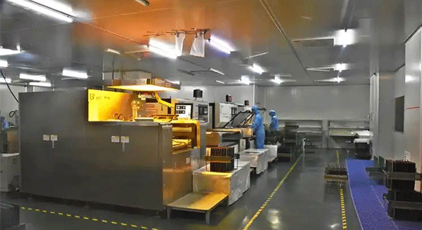
Formal semiconductor-grade etching production is carried out in a clean workshop, and the finished parts are cleaned with multi-stage deionized water to strictly control the number of surface residual particles, meeting the cleanliness requirements of semiconductor packaging scenarios. No foreign matter remains on the surface of the finished parts, which avoids the risk of chip pollution and failure caused by impurities in the subsequent packaging process, and adapts to the high-standard quality management system of the semiconductor industry.
7. Wide Compatibility with Semiconductor Special Alloys
In addition to conventional copper and stainless steel, the process is also compatible with various special alloys for semiconductors such as Kovar alloy, molybdenum-copper, Invar and nickel-based alloy. Special etchant formulations are developed for different materials to ensure uniform etching rate and high surface quality, while fully retaining the unique thermal expansion, electrical conductivity and heat resistance properties of each alloy, meeting the material requirements of different packaging scenarios.
II. Core Functions & Industrial Value in Semiconductor Manufacturing
As a key supporting process for semiconductor packaging, metal etching delivers six core functional values, solving multiple pain points in traditional semiconductor metal component processing.
1. High-Density Lead Frame Precision Forming
The most core function is to manufacture integrated circuit lead frames, realizing high-density arrangement of chip pins, and ensuring the accuracy and consistency of electrical connection paths. Compared with stamping processes, etching is more suitable for fine-pitch, high-density packaging forms, and will not cause pin deformation and burr problems, effectively improving packaging yield and electrical performance stability.
2. Integrated EMI Shielding Component Fabrication
Metal etching can integrally form ultra-thin EMI shielding covers and shielding frames for chip-level packaging. The integrated structure has no splicing gaps, with better electromagnetic shielding effect, and the ultra-thin material adapts to the miniaturization requirements of system-in-package (SiP). The stress-free flat structure ensures close fitting with the package body, avoiding signal interference and improving the operation stability of high-frequency chips.
3. Micro-Structure Processing for Heat Dissipation Components
It is used to process the metal wick structure of VC vapor chambers and heat pipes for high-power chips. The uniform micro-hole array structure provides stable capillary force, improves heat conduction efficiency, and solves the heat management problem of high-power computing chips and radio frequency chips. The etching process can realize complex multi-stage wick structures, which is difficult to achieve by stamping processes, and effectively improves the heat dissipation performance of the package.
4. High-Reliability Ceramic Package Metal Parts Forming
For high-reliability ceramic packaging scenarios such as aerospace and automotive electronics, metal etching processes metal cover plates, lead rings and electrode base parts matching ceramic packaging. The high dimensional accuracy ensures the airtightness of the package, and the stress-free structure will not affect the long-term reliability of the package, meeting the use requirements of extreme environments such as high temperature, vibration and corrosion.
5. Rapid Prototyping to Accelerate Packaging R&D Iteration
The low-cost digital mask of metal etching enables rapid prototype delivery within 24–48 hours, supporting packaging design teams to quickly verify different structural schemes. There is no expensive mold development cost, which greatly reduces the trial-and-error cost of new product R&D, shortens the overall R&D cycle of chip packaging products, and helps products seize the market faster.
6. Optimize Supply Chain Cost and Improve Production Efficiency
Compared with the stamping process which requires high mold costs, metal etching saves expensive mold investment for small and medium batch orders, and has higher yield for complex fine structures. For mass production, automated lines have high production efficiency and stable quality, which comprehensively reduces the total procurement cost of semiconductor metal parts and optimizes the efficiency of the entire packaging supply chain.
III. Key Application Scenarios in the Semiconductor Industry
With its unique technical advantages, metal etching has been widely used in multiple links of the semiconductor industry chain from packaging to equipment manufacturing.
1. IC Packaging Lead Frames
This is the most core application field of semiconductor metal etching. It is suitable for high-density packaging forms such as QFP, SOP and QFN, as well as lead frames for discrete devices, analog chips and power devices. It supports finer pin pitch and higher integration density, and is an important supporting process for the development of advanced packaging toward miniaturization.
2. Chip-Level EMI Shielding Components
It is widely used in consumer electronics chips, radio frequency chips and system-in-package EMI shielding covers, shielding frames and partition structures. Ultra-thin forming and high dimensional accuracy meet the shielding requirements of high-density miniaturized packaging, and effectively suppress electromagnetic crosstalk between chips.
3. Advanced Packaging Heat Dissipation Structures
For high-power chips such as AI computing chips, 5G radio frequency chips and power semiconductors, it processes the wick structure inside VC vapor chambers and flat heat pipes, improves the heat dissipation capacity of the package, solves the thermal management bottleneck of high-power chips, and supports the continuous improvement of chip power density.
4. High-Reliability Ceramic Packaging Parts
In aerospace, military and automotive-grade high-reliability packaging, it is used to manufacture metal cover plates, electrode leads and sealing rings for ceramic packages. It has high airtightness matching accuracy and stable material properties, ensuring the long-term reliable operation of chips in extreme environments such as high and low temperature, strong vibration and corrosion.
5. MEMS Device Precision Metal Structures
It is used to process precision metal components for MEMS sensors, micro-actuators and micro-fluidic chips. The micro-structure has high precision and no residual stress, which will not affect the sensitive performance of MEMS devices, and meets the processing requirements of micro-electromechanical systems for ultra-fine structures.
6. Semiconductor Equipment Precision Fittings
It provides precision metal shims, positioning fixtures, mask accessories and micro-structural parts for wafer manufacturing and packaging equipment. The high dimensional accuracy ensures the operation accuracy of the equipment, and the stable batch consistency supports the long-term stable operation of the production line, meeting the high-precision requirements of semiconductor manufacturing equipment.
7. Power Semiconductor Connection Components
For power devices such as IGBT and MOSFET, it processes insulating gaskets, connecting electrodes and heat dissipation structural parts. It retains the excellent electrical and thermal conductivity of the base material, adapts to the working scenario of high voltage and large current, and improves the operation stability and service life of power semiconductor devices.
Conclusion
In summary, the metal etching process has become an indispensable precision manufacturing technology in the semiconductor industry chain with its core advantages of micron-level precision, stress-free burr-free forming, ultra-thin material adaptability and stable mass production capacity. It strongly supports the development of semiconductor packaging toward higher density, thinner size and higher reliability, and plays a key role in lead frame manufacturing, electromagnetic shielding, heat dissipation structure and other links.
With the continuous development of advanced packaging, Chiplet technology and high-power chips, the market demand for high-precision semiconductor metal components will continue to grow. In the future, the metal etching process will continue to evolve toward higher precision, thinner materials and higher cleanliness standards, providing more solid technical support for the iterative upgrading of the semiconductor industry.