Photo Etching on Metal: Precision Process, Benefits & Industrial Applications
Photo etching on metal, also known as photochemical etching (PCM) or metal chemical etching, is an advanced non-contact cold subtractive manufacturing technology that transfers pre-designed geometric patterns onto metal substrates through UV photolithography and controlled chemical corrosion. Unlike traditional stamping, laser cutting and CNC milling that rely on mechanical force or high-temperature energy to remove materials, metal photo etching forms parts through uniform molecular-level chemical dissolution at room temperature, delivering burr-free edges, zero residual stress and micron-level dimensional accuracy.
As global manufacturing continues to pursue component miniaturization, higher performance reliability and faster product iteration, photo etching has become an indispensable processing solution for high-end precision metal parts. It effectively solves the inherent defects of traditional processes such as deformation, burrs and high tooling costs for thin-walled and complex-structured parts, and is widely recognized and adopted in high-precision manufacturing fields such as electronics, aerospace, medical devices and new energy.
I. Key Characteristics of Photo Etching on Metal
The unique room-temperature chemical forming mechanism gives metal photo etching a series of core advantages that traditional processing technologies cannot match. These characteristics run through the entire product lifecycle from prototyping to mass production, directly determining the performance, cost and delivery efficiency of final parts.
1. Stress-Free Cold Processing & Full Material Property Retention
As a room-temperature cold processing technology, photo etching applies no mechanical extrusion force, punching impact or high-temperature thermal impact to the metal substrate, and does not generate residual internal stress, lattice deformation or material property changes inside the material. Stamped parts typically carry large residual stresses that gradually release during temperature cycling and long-term service, causing dimensional drift and fatigue fracture; laser-cut parts have obvious heat-affected zones that reduce material corrosion resistance and fatigue strength.
Photo-etched metal parts fully retain the original mechanical, physical and chemical properties of the base material, with zero degradation in elasticity, conductivity, corrosion resistance and fatigue strength. This feature is particularly critical for high-reliability scenarios such as aerospace springs, medical implants and electronic signal components, and can extend the service life of parts by more than 3 times compared with stamping and laser processes.
2. Micron-Level Precision & Complex Geometry Freedom
Precision photo etching achieves a stable dimensional tolerance of ±0.005mm to ±0.01mm, with a minimum machinable line width of 0.02mm, and the minimum machinable aperture is approximately 1.1 times the material thickness according to mature process rules. There is no restriction on graphic complexity: arbitrary curves, hollow patterns, multi-track composite structures and micro-grating arrays can be formed in one process, and the complexity of the pattern does not increase the processing cost.
For complex parts such as encoder discs, multi-finger spring contacts and micro-filter arrays, traditional processes require multiple processing steps with cumulative errors, while photo etching completes all features in a single forming step with high pattern fidelity. Designs optimized by optical simulation, fluid dynamics simulation and mechanical simulation can be reproduced 1:1 without process constraints, giving engineers maximum design freedom.
3. Burr-Free Smooth Edges & No Secondary Deburring
Photo etching removes metal through uniform chemical dissolution, forming smooth, vertical and rounded edges completely free of burrs, flanging, tool marks and sharp protrusions. Stamping, punching and CNC machining inevitably produce burrs on part edges, requiring secondary deburring processes that increase costs and easily damage the dimensional accuracy of thin parts. Sharp burrs can also scratch mating surfaces, accelerate wear, and shed micro-debris that contaminates sensitive systems such as semiconductors and medical devices.
The burr-free feature eliminates the need for post-processing deburring, reduces production procedures and costs, and avoids particulate shedding risks during product operation. It is an essential requirement for high-cleanliness and high-safety application scenarios such as medical equipment, food contact parts and semiconductor components.
4. Tooling-Free Rapid Prototyping & Low Customization Cost
Unlike stamping which requires expensive hard steel dies with a production cycle of tens of days and a cost of thousands to tens of thousands of dollars, photo etching uses digital photomask films as tooling. The production cost of a single photomask is less than 1/50 of that of a stamping die, and the production cycle is only a few hours. Design modifications only need to adjust the electronic drawing file and re-output the photomask, with no additional mold modification costs.
Prototype samples can be delivered within 24–48 hours after drawing confirmation, greatly shortening the product R&D cycle and reducing trial-and-error costs. From 1–10 pieces of laboratory prototype samples to millions of pieces of mass production, the process covers the full demand range without minimum order threshold, which is very suitable for the current market trend of multi-variety and small-batch customized manufacturing.
5. Broad Material Compatibility Across Engineering Metals
Photo etching is compatible with almost all common engineering metal materials, including 304/316L stainless steel, beryllium copper, phosphor bronze, pure copper, titanium alloy, nickel alloy, Invar, Hastelloy, Monel and molybdenum. Dedicated etchant formulas and process parameters are developed for different materials to ensure uniform etching rate and high-quality forming effect, while fully retaining the native properties of each material.
Highly reflective materials such as copper and aluminum, which are difficult to process by laser cutting, can be stably etched without energy loss; brittle and hard alloys that are easy to crack during stamping can also be formed without damage. Customers can select the most suitable material according to product performance requirements, without being restricted by processing technology.
6. High Batch Consistency & Stable Mass Production Quality
Photo etching relies on digital photomask imaging and uniform chemical reaction, ensuring that every part on the same processing sheet has identical dimensions, shape and performance. Automated closed-loop production lines with constant temperature and concentration control achieve highly consistent quality across mass production batches, with dimensional uniformity above 99.5% and a comprehensive yield rate stable above 98.5%.
Compared with stamping, which suffers from gradual tool wear and quality drift during long-term mass production, photo etching maintains completely consistent accuracy from the first part to the millionth part. There is no mold wear and maintenance cost, and the long-term mass production quality stability is significantly better than traditional mechanical processing.
7. Uniform Full-Sheet Processing & High Material Utilization
Photo etching processes the entire metal sheet at the same time, and can typeset multiple models and multiple parts on the same sheet for simultaneous processing, greatly improving production efficiency. The edge waste of the sheet is small, and the material utilization rate can reach more than 80%, which is significantly higher than the material utilization rate of CNC milling and laser cutting. For precious metal materials such as titanium alloy and nickel alloy, high material utilization rate can greatly reduce raw material costs.
II. Core Functions of Photo-Etched Metal Components
As a precision manufacturing process, photo etching on metal undertakes six core functional values for downstream products, providing fundamental support for product performance improvement, cost optimization and innovation breakthrough.
1. Precision Functional Pattern Integration
The most core function of photo etching is to integrate high-precision functional patterns directly on a single piece of metal sheet, including conductive circuits, sensing gratings, micro-hole arrays, elastic structures and sealing profiles, so that a single thin metal part can simultaneously realize multiple functions such as electricity, optics, fluid and machinery. It eliminates the need for multi-part assembly, reduces overall product volume and improves structural reliability.
2. High-Accuracy Dimensional Guarantee for Precision Assembly
Micron-level forming accuracy and stress-free dimensional stability ensure that etched parts can achieve high-precision matching with mating components, reduce assembly gaps and tolerance accumulation, and improve the overall assembly accuracy and operational stability of equipment. For precision mechanisms such as optical instruments and semiconductor equipment, stable dimensional accuracy directly determines the working accuracy and repeatability of the whole machine.
3. Surface Integrity Protection for High Reliability
By preserving complete material properties and surface integrity, photo etching eliminates internal defects such as residual stress and micro-cracks introduced by traditional processes, greatly improving the long-term reliability and fatigue life of parts. For mission-critical products in aerospace, medical and other fields, surface integrity directly determines product safety and service life, and is a core indicator that cannot be compromised.
4. Flexible Customization to Accelerate Innovation
Low-cost and fast prototyping capabilities support enterprises to quickly verify new design solutions, shorten the R&D cycle of new products, and reduce R&D investment risks. Enterprises can launch differentiated products more quickly according to market demand changes, improving market response speed and product competitiveness. This is particularly important in fast-updating industries such as consumer electronics and new energy.
5. Scalable Production Matching Full Lifecycle
From R&D prototype trial production to medium-volume climbing production and then to large-scale mass production, the photo etching process can seamlessly connect, without the need to re-develop processes and replace processing methods when scaling up production. The product performance and quality are completely consistent from prototype to mass production, avoiding the performance deviation and secondary verification costs caused by process replacement.
6. Clean Processing for Hygiene-Sensitive Scenarios
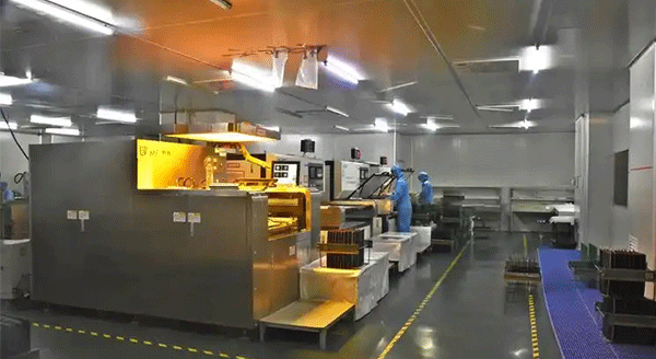
The whole etching process is completed in a clean workshop. After multi-stage ultrasonic cleaning and vacuum drying, the finished parts have no oil stains, debris and chemical residues, reaching electronic-grade and medical-grade cleanliness. There is no stamping oil residue and laser oxide dust pollution, which can directly enter the assembly link of high-end industries such as medical treatment, semiconductors and food, reducing customers’ post-cleaning costs and quality risks.
III. Main Industrial Applications of Photo Etching on Metal
Driven by the global precision manufacturing upgrading trend, photo etching technology is expanding into more and more high-end industrial fields, and its application scope covers almost all industries that require precision metal parts.
1. Electronics & Semiconductor Manufacturing
This is the largest application field of metal photo etching. Etched parts include semiconductor lead frames, EMI shielding cans, heat pipe vapor chamber wicks, connector spring contacts and flexible circuit substrates. Its micron-level precision, burr-free quality and stress-free structure perfectly match the development trend of high-density, miniaturized and high-reliability electronic components, and are core processing technology for mid-to-high-end electronic components.
2. Aerospace & Defense Aviation
In the aerospace field, photo etching is used to manufacture precision shims, filter screens, elastic contacts, sensor components and heat dissipation parts for aircraft, satellites and missile systems. Its advantages of full material property retention, stress-free stability and high fatigue reliability meet the ultra-high reliability requirements of aerospace products, and can adapt to extreme working environments such as wide temperature range, strong vibration and high altitude.
3. Medical Devices & Biotechnology
Medical-grade photo-etched parts include surgical instrument components, implantable electrodes, infusion filter meshes, biosensor chips and orthodontic brackets. The burr-free, clean and biocompatible characteristics fully comply with strict medical safety standards, and can withstand high-temperature and high-pressure sterilization without performance degradation, providing reliable support for medical device safety and efficacy.
4. Automotive & New Energy Vehicles
In the automotive industry, photo etching is used to produce encoder discs for automotive motors, transmission filter meshes, battery pack current collectors, hydrogen fuel cell bipolar plates and connector shrapnel. Its high batch consistency and long-term stability meet the strict quality requirements of the automotive industry, and adapt to the complex vehicle operating environment of vibration, temperature difference and corrosion.
5. Industrial Automation & Motion Control
Photo-etched encoder discs, precision shims, flat springs and filter screens are widely used in servo motors, CNC machine tools, industrial robots and automated production lines. High-precision grating and stress-free structure ensure stable and reliable motion control feedback, and are key basic components to ensure the operation accuracy and stability of automation equipment.
6. Energy & Environmental Protection
In the new energy and environmental protection fields, photo etching is used to manufacture fuel cell bipolar plates, electrolyzer electrode components, industrial filter screens and water treatment filter elements. Its excellent corrosion resistance and precise flow control capabilities adapt to the harsh working environment of energy equipment, and help improve energy conversion efficiency and equipment service life.
7. Consumer Electronics & Precision Hardware
Consumer electronics products such as smartphones, headphones and wearable devices use a large number of photo-etched parts, including speaker dust meshes, camera VCM springs, SIM card contacts, button shrapnel and decorative hollow parts. Ultra-thin forming, complex pattern and high mass production consistency perfectly match the demand characteristics of consumer electronics such as lightness, refinement and large-scale supply.
Conclusion
With the continuous upgrading of global high-end manufacturing and the accelerated iteration of downstream products such as new energy, semiconductors and consumer electronics, the market demand for high-precision, high-quality and fast-delivered precision metal parts continues to grow. Photo etching on metal, with its unique advantages of stress-free cold processing, micron-level accuracy, burr-free forming, flexible customization and cost-effective mass production, has gradually become a mainstream precision manufacturing process, replacing more and more traditional stamping and laser processing scenarios.
As an important part of the advanced manufacturing system, metal photo etching technology will continue to develop in the direction of higher precision, wider material adaptation and more intelligent production, providing stronger technical support for the innovation and upgrading of various high-end manufacturing industries, and has broad market development prospects and application value.