
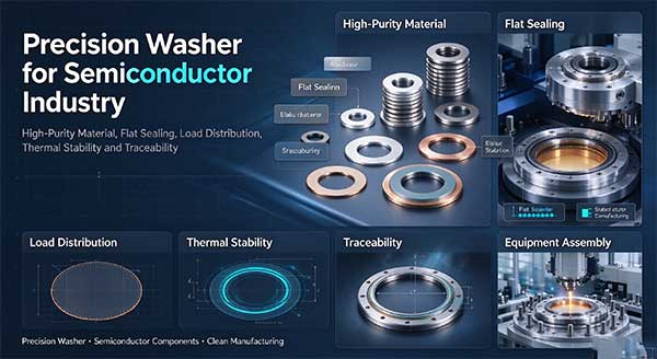
custom etched washer
Precision washers are critical thin metal components widely applied across the semiconductor industry for wafer processing equipment, vacuum chambers, lithography machines, test fixtures and chip packaging assemblies. These ultra-flat washers function as spacing, leveling, sealing and load-distributing parts to maintain stable assembly clearance under high vacuum, high temperature and cleanroom operating environments.
Semiconductor-grade precision washers require extremely strict flatness and dimensional tolerance. Even tiny deformation, burrs or surface particles may contaminate wafers, disrupt optical alignment and cause equipment downtime. Photo chemical etching is the preferred manufacturing method for ultra-thin semiconductor washers, as it delivers burr-free, stress-free parts without mechanical stamping deformation.
A wide range of high-purity metals can be used for semiconductor precision washers, including stainless steel, nickel, copper, titanium and kovar alloy. Material selection depends on working conditions such as vacuum level, corrosive gas exposure, temperature fluctuation and electrical conductivity requirements. Etched precision washers support custom outer diameter, inner hole and thickness, even for foil thickness below 0.1mm.
Main Applications of Semiconductor Precision Washers
- Wafer carrier & fixture assembly: Fine spacing adjustment during wafer holding and inspection
- Vacuum chamber components: Flat sealing shims for semiconductor vacuum systems
- Lithography & optical equipment: Leveling washers to keep optical path alignment
- Chip packaging fixtures: Thin washers for packaging tool preload and gap control
- Semiconductor test sockets: Small precision washers for contact assembly calibration
Key Requirements & Benefits
- Ultra tight tolerance: Controlled OD, ID and thickness to meet micron-level assembly needs
- Burr-free & stress-free: No sharp edges or residual stress to avoid particle generation in cleanroom
- Excellent flatness: Prevents uneven pressure that damages delicate wafers and optical parts
- Clean surface finish: Easy cleaning to satisfy semiconductor cleanroom standards
- Low tooling cost: Fast prototype turnaround, suitable for small batch custom development
Compared with stamped washers, chemically etched precision washers avoid burrs and material deformation. Laser cutting may introduce heat-affected zones on thin foils, which is not acceptable for high-end semiconductor equipment. PCM etching can produce thin washers with consistent flatness and repeatability from prototype to mass production.
We provide custom precision washer manufacturing service for semiconductor customers. We verify CAD drawings, control flatness and dimensional tolerance strictly, and implement rigorous cleaning and inspection before shipment for all semiconductor metal washers.