
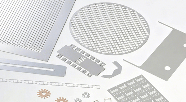
Stainless Steel Etching Process: Steps, Features & Industrial Applications
The stainless steel etching process, also widely known as photochemical machining, is a precision cold working manufacturing technology that uses photolithography masking and controlled chemical corrosion to remove redundant material from stainless steel substrates. Different from stamping, laser cutting and CNC milling which rely on mechanical extrusion or thermal ablation, stainless steel etching removes metal at the molecular level through homogeneous liquid-phase chemical reactions. It effectively overcomes common defects such as material deformation, work hardening, thermal oxidation and edge burrs caused by traditional processing methods.
Applicable to almost all mainstream stainless steel grades including 201, 304, 316L, 321 and duplex stainless steel, the stainless steel etching process can handle ultra-thin foils as thin as 0.01mm up to medium-thickness plates of 2mm. Thanks to its high dimensional repeatability, stress-free forming and tooling-free customization, it has become the preferred production solution for high-precision stainless steel micro-components, deeply applied in high-end manufacturing fields such as electronic packaging, medical devices, aerospace and new energy equipment.
1. Standard Step-by-Step Workflow of Stainless Steel Etching Process
The whole stainless steel etching process follows a closed-loop standardized production route, with parameters adjusted according to material thickness, alloy composition and required etching depth to guarantee stable quality in mass production.
1.1 Surface Pre-treatment and Degreasing
Stainless steel surfaces easily form oil stains, fingerprints and dense passive oxide films during storage and transportation, which will lead to uneven photoresist adhesion and inconsistent etching depth. The pre-treatment stage includes ultrasonic degreasing to eliminate organic contaminants, weak acid pickling to remove natural oxide layers, and micro-roughening treatment to form a tiny uniform textured surface. This step greatly improves the bonding force between the base material and the subsequent photoresist layer, avoiding pattern warping and edge distortion during etching.
1.2 Photoresist Coating and UV Exposure
A uniform layer of UV-sensitive dry film or liquid photoresist is coated on the cleaned stainless steel surface, with coating thickness matched to the target etching depth. A high-precision photographic mask carrying the designed graphic layout is precisely aligned on the workpiece, followed by controlled ultraviolet exposure. The exposed area of the photoresist undergoes photopolymerization to form a corrosion-resistant protective layer, while the unexposed area remains soluble for subsequent development. For ultra-thin stainless steel foils, low-energy exposure parameters are adopted to prevent substrate penetration damage.
1.3 Development and Thermal Curing
After exposure, the unpolymerized photoresist is washed away by alkaline developer solution, accurately transferring the target graphic pattern onto the protective film. The workpiece then enters a low-temperature baking oven for curing treatment, which further strengthens the corrosion resistance and adhesion of the remaining photoresist mask, ensuring it will not be eroded or peeled off during long-time immersion in the etching solution.
1.4 Controlled Chemical Etching Reaction
This is the core link of the stainless steel etching process. The cured semi-finished product is conveyed into an automatic spraying etching tank, where ferric chloride-based acidic etching solution is evenly sprayed on both sides of the workpiece. By precisely locking three core variables — etchant concentration, constant temperature and spraying pressure — the exposed stainless steel area is selectively dissolved and removed. For thin foils, low-concentration potion and short processing time are used to prevent over-etching and wrinkling; for thick plates, the side etching ratio is strictly controlled to ensure high pattern fidelity.
1.5 Photoresist Stripping and Passivation Post-treatment
Once the preset etching depth or through-cutting effect is achieved, the workpiece is sent to the stripping station to completely remove the residual photoresist mask with alkaline stripping liquid. Multiple cycles of pure water rinsing are carried out to wash away residual etching chemicals. Finally, surface passivation treatment is performed to rebuild a compact anti-rust passive film on the stainless steel surface, preventing oxidation discoloration and improving long-term corrosion resistance of finished parts.
1.6 Dimensional Inspection and Protective Packaging
Finished stainless steel components undergo full inspection with optical measuring instruments, covering dimensional tolerance, edge smoothness, etching depth and surface flatness. Qualified products are dried and packed with anti-scratch, anti-oxidation packaging materials to avoid scratching and contamination during storage and transportation.
2. Core Technical Features of Stainless Steel Etching Process
2.1 Room-temperature Stress-Free Cold Processing
The entire stainless steel etching process is completed in a liquid environment at normal temperature, without any mechanical impact and thermal input. It will not cause foil tearing, edge curling and internal residual stress like stamping, nor produce heat-affected zones and edge embrittlement like laser cutting. The original mechanical strength, elasticity and corrosion resistance of stainless steel are 100% retained, which is especially critical for elastic shrapnel and ultra-thin functional components.
2.2 Burr-Free Smooth Edges Without Secondary Finishing
Material removal relies on molecular uniform dissolution, resulting in smooth, rounded and transitionally natural edges without burrs, molten slag and sharp protrusions. Most etched parts can be directly assembled without deburring, grinding and polishing procedures, reducing post-processing labor costs and eliminating hidden dangers such as circuit short-circuit and filter blockage caused by loose metal particles.
2.3 Micron-level High Precision and Full-Sheet Uniformity
Mature stainless steel etching technology can control the dimensional tolerance of thin foils within ±0.005mm and medium plates within ±0.02mm. All graphic features on the whole sheet are formed simultaneously through chemical reaction, without cumulative positioning errors of point-by-point processing. The dimensional consistency rate of mass production exceeds 99.5%, meeting the strict precision requirements of micro holes, dense grid arrays and encoder discs.
2.4 Accurate Half-Etching Integrated Molding
A unique advantage of the stainless steel etching process is controllable half-etching partial depth processing. The etching depth can be locked within ±0.003mm for thin materials, enabling one-step integrated production of positioning grooves, step platforms, bending indentations and anti-slip textures on a single stainless steel sheet. It avoids the positioning deviation caused by secondary machining and improves assembly matching accuracy.
2.5 Tooling-Free Design Freedom and Low Iteration Cost
No hard metal molds are required for stainless steel etching. Complex curves, irregular outlines, variable-density hole arrays and personalized decorative patterns can all be produced directly from CAD drawings. Design revisions only need to update the photomask file, without expensive mold opening fees and long debugging cycles, greatly supporting small-batch customized orders and rapid prototype verification.
2.6 Wide Compatibility of Stainless Steel Grades and Thicknesses
The process is adaptable to a full range of stainless steel alloys from austenitic 304/316L to ferritic and duplex grades. The applicable thickness covers 0.01mm ultra-thin foil to 2mm thick plate. Different etching solution formulas are matched according to alloy corrosion resistance, realizing stable etching quality for hard, corrosion-resistant stainless steel materials that are difficult for mechanical cutting.
2.7 Stable Batch Repeatability for Mass Production
The automatic closed-loop production line monitors and compensates etchant concentration, temperature and spraying pressure in real time. Without tool wear and loss, the product quality remains consistent from the first batch to tens of thousands of batches, effectively avoiding quality drift and satisfying the batch traceability standards of automotive, medical and aerospace industries.
3. Core Functional Value of Stainless Steel Etching Process
3.1 Precision Microstructure Forming
The most basic function is to accurately transfer digital design patterns into physical microstructures, producing micro filter meshes, fine grid shielding nets, elastic contact shrapnels and precision gaskets that cannot be efficiently manufactured by traditional processes, supporting the miniaturization trend of modern industrial products.
3.2 High Cleanliness and High Reliability Component Manufacturing
Burr-free, particle-free and stress-free finished surfaces meet the high cleanliness standards of semiconductor packaging and medical equipment. The complete retention of stainless steel’s anti-corrosion performance ensures long-term stable operation of parts in humid, salt spray and weak acid environments, lowering product failure rates.
3.3 Agile R&D Iteration and Rapid Prototyping
Low-cost photomask proofing shortens the sample delivery cycle to 24–48 hours, helping designers quickly verify multiple structural schemes, greatly reducing R&D trial-and-error costs and shortening the overall product launch cycle.
3.4 Integrated Multi-Functional One-Step Molding
Multiple functional structures such as through holes, positioning notches, half-etched grooves and elastic cantilevers can be integrated on one stainless steel workpiece in a single process, replacing multi-piece assembly structures, reducing overall volume and improving structural stability.
3.5 Optimized Total Lifecycle Manufacturing Cost
Although the unit price of single-piece processing is higher than large-volume stamping, stainless steel etching saves mold investment, reduces secondary finishing procedures and improves the yield rate of thin materials. For small and medium batches, customized parts and complex graphic products, the comprehensive manufacturing cost has obvious advantages.
3.6 Environmentally Friendly Closed-Loop Production
Modern production lines are equipped with etching solution filtration, regeneration and waste liquid treatment systems. The etchant can be recycled and replenished for repeated use, reducing chemical consumption and pollutant discharge, complying with global green manufacturing and environmental protection compliance requirements.
4. Main Industrial Application Fields
4.1 Electronics and Semiconductor Packaging
The largest application scenario. The stainless steel etching process produces EMI shielding covers, ultra-thin heat dissipation grids, wafer carrier fixtures, micro connector shrapnels and lead frame auxiliary parts. High precision and burr-free features match the high-density and miniaturization needs of chip packaging.
4.2 Medical Devices and Life Sciences
304 and 316L medical-grade etched stainless steel components include infusion filter screens, surgical instrument accessories, cell sieve plates and implant auxiliary structural parts. Smooth edges avoid tissue scratches, and the material can withstand repeated high-temperature sterilization, meeting strict medical biocompatibility standards.
4.3 Aerospace and High-End Precision Equipment
Etched parts such as ultra-thin precision shims, hydraulic micro filter screens, lightweight ventilation grids and sensor diaphragms are widely used in aerospace equipment. Stress-free processing retains fatigue resistance and corrosion resistance, adapting to extreme working conditions of large temperature differences and strong vibration.
4.4 New Energy and Automotive Electronics
Used for new energy battery heat dissipation meshes, fuel cell auxiliary flow field plates, vehicle sensor shrapnels, battery pack ventilation protection nets and automotive precision gaskets. Stable batch performance meets automotive-grade long-term reliability requirements.
4.5 Precision Instruments and Optoelectronic Equipment
Manufactures optical slits, encoder grating discs, precision diaphragms and light barrier sheets for spectrometers, laser equipment and testing instruments. Micron-level edge accuracy eliminates stray light and diffraction interference, guaranteeing stable detection accuracy of precision instruments.
4.6 Industrial Filtration and Environmental Protection Equipment
Various etched stainless steel filter elements, hydraulic oil filter screens and water treatment perforated plates are applied in chemical industry, food processing and water purification systems. Uniform aperture ensures stable filtration accuracy and anti-clogging performance.
4.7 Architectural Decoration and High-End Hardware
Custom etched patterns, texture logos and hollow decorative panels are used for building curtain walls, interior partitions and high-end hardware accessories, utilizing delicate etching lines to enhance the decorative texture and product added value.
Conclusion
In conclusion, the stainless steel etching process is a mature and reliable precision cold working technology that perfectly solves the processing pain points of ultra-thin stainless steel sheets and complex micro-components. With core strengths including stress-free forming, burr-free edges, micron-level dimensional accuracy, wide material adaptability and tooling-free customization, it fills the production gap that traditional stamping, laser cutting and CNC machining cannot cover.
As downstream industries continuously raise requirements for component miniaturization, surface cleanliness and long-term reliability, the market demand for high-precision etched stainless steel parts will keep expanding. In the future, the stainless steel etching process will continue to upgrade toward higher etching resolution, more environmentally friendly potion formulas and intelligent automatic parameter adjustment, providing more solid processing support for product innovation and quality upgrading in electronics, medical treatment, aerospace, new energy and other high-end manufacturing sectors.