
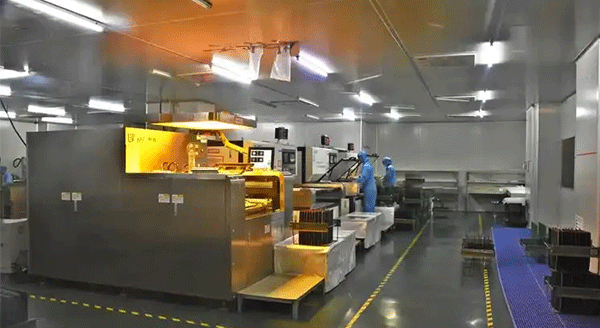
Wet Chemical Etching in Semiconductor Manufacturing
Wet chemical etching is a foundational core process in semiconductor wafer fabrication. It achieves selective material removal through controlled chemical reactions between liquid etchants and thin-film materials on the wafer surface, serving as a critical step for photolithography pattern transfer, surface cleaning and microstructure fabrication. While dry plasma etching dominates advanced-node processes below 28nm, wet chemical etching retains irreplaceable value in mature nodes, power devices, MEMS and advanced packaging due to its unique advantages of ultra-high etch selectivity, zero plasma damage and low-cost batch processing. It remains an indispensable part of the complete semiconductor manufacturing process system.
Different from mechanical and plasma-based dry processing, wet etching relies entirely on room-temperature or low-temperature liquid-phase chemical reactions to shape structures. It does not require high-vacuum environments, high-energy ion beams or complex RF systems, and has a longer development history with a more mature and stable process system. With the rapid growth of power semiconductors, MEMS and third-generation compound semiconductors, the application scale of wet chemical etching continues to expand, playing an increasingly important role in the entire semiconductor industry chain.
I. Core Characteristics of Wet Chemical Etching in Semiconductor Manufacturing
The liquid-phase chemical reaction mechanism endows wet etching with a series of unique technical attributes that dry etching cannot replicate. These characteristics determine its irreplaceable position in specific semiconductor manufacturing scenarios.
1. Isotropic Etching with Ultra-High Uniformity
Wet chemical etching is a typical isotropic process: the etchant corrodes the target material at the same rate in all directions, achieving extremely high etching uniformity across the entire wafer surface. For 12-inch wafers, the within-wafer etch thickness deviation can be controlled within ±1%, which is significantly better than the uniformity level of dry plasma etching.
This uniform etching characteristic is particularly suitable for full-wafer thin-film thinning and surface smoothing processes. It can also form curved, spherical and horn-shaped microstructures that cannot be achieved by anisotropic dry etching, such as microlens arrays and microfluidic cavities, providing unique structural forming capabilities for optoelectronic and biochip devices.
2. Ultra-High Etch Selectivity
High selectivity is the most prominent advantage of wet chemical etching. By optimizing etchant formulation, pH value and temperature, extremely high etch rate ratios can be achieved between the target material and the mask layer (photoresist, hard mask) and the underlying substrate. For example, buffered oxide etch (BOE) can achieve a selectivity of more than 100:1 between silicon dioxide and photoresist, and an even higher selectivity between silicon dioxide and silicon substrate.
This high selectivity ensures that the etching process hardly damages the mask and underlying functional layers, can accurately retain the designed pattern structure, and is suitable for processing ultra-thin films and multi-layer stacked structures. It avoids device performance failures caused by over-etching, and significantly improves process tolerance and product yield.
3. Zero Plasma Damage & Stress-Free Processing
As a pure chemical reaction process, wet etching involves no ion bombardment, high-energy radiation or charge accumulation, and will not cause lattice damage, dangling bonds or surface defect layers on the wafer surface. It also does not introduce residual stress into the material, fully preserving the original electrical, optical and mechanical properties of the semiconductor material.
For power devices, optoelectronic components and ultra-thin wafers that are extremely sensitive to processing damage, wet etching can effectively avoid problems such as increased leakage current and reduced breakdown voltage caused by dry etching damage, and significantly improve device reliability and service life. This is the core reason why wet etching remains irreplaceable in power semiconductor manufacturing.
4. High-Throughput Batch Processing
Wet etching systems mostly adopt tank-based or spray batch processing architecture, which can process 25 or more wafers at a time. Its throughput per unit time is much higher than single-wafer dry etching equipment. For mass production at mature process nodes, the processing cost per wafer of wet etching is only 1/3 to 1/5 of that of dry etching, with significant cost advantages.
This batch processing capability perfectly matches the large-scale mass production demand of mature-node chips, discrete devices and optoelectronic components, and is the preferred etching solution for cost-sensitive mass production scenarios.
5. Broad Material Compatibility
A complete mature etchant system has been formed for almost all mainstream semiconductor materials. Buffered oxide etch (BOE/BHF) is used for silicon dioxide etching; phosphoric acid solution is used for aluminum metal interconnect etching; KOH/TMAH is used for anisotropic etching of monocrystalline silicon; nitric-acetic acid mixed solution is used for polysilicon etching; aqua regia system is used for noble metal electrode etching.
From elemental silicon and compound semiconductors to dielectric layers and metal layers, wet etching covers almost all mainstream material systems in semiconductor manufacturing. For new compound semiconductor materials such as SiC and GaN, dedicated wet etchant formulations are also being rapidly improved.
6. Stable Process Consistency
Modern automated wet etching equipment is equipped with precision temperature control, real-time concentration monitoring, closed-loop timing and automatic reagent replenishment systems, and the etch rate fluctuation can be controlled within ±2%. The fully enclosed automated process environment avoids pollution and errors caused by manual intervention, and achieves extremely high dimensional consistency between batches.
This stable process repeatability meets the strict process control standards of the semiconductor industry, supports long-term stable mass production, and reduces the quality fluctuation risk in the production process.
7. Low Equipment & Maintenance Cost
Wet etching equipment does not require complex systems such as high vacuum chambers and high-frequency power supplies, and its equipment procurement and maintenance costs are much lower than those of dry etching machines. At the same time, the wet etching process has a long development history, a mature and stable process system, and a complete supporting chemical supply chain, which shortens the process development cycle and reduces the construction threshold of wafer fabrication lines.
II. Core Functions of Wet Chemical Etching in Semiconductor Fabrication
Wet chemical etching undertakes six core functional roles in the semiconductor manufacturing process chain, which are the key guarantees for device performance, yield and manufacturing cost.
1. Precision Pattern Transfer & Thin Film Patterning
This is the most core function of wet etching in front-end manufacturing. After the photolithography process is completed, wet etching selectively dissolves the exposed thin-film material, accurately transfers the design pattern on the photoresist to the functional thin-film layer of the wafer, and realizes key patterning steps such as dielectric layer window opening, metal interconnection forming and doping region masking.
With the support of high selectivity, pattern transfer fidelity is high, which is the core process link of front-end manufacturing at mature process nodes. For aluminum interconnection, passivation layer and other structures, wet patterning still has better cost performance and reliability than dry etching.
2. Wafer Surface Cleaning & Pre-Treatment
Wet cleaning, as a mild form of wet etching, is the process with the most steps and the highest frequency in semiconductor manufacturing. Represented by RCA standard cleaning, wet cleaning processes remove particle contamination, metal impurities, native oxide layers and organic residues on the wafer surface through different chemical reagent combinations, providing a clean surface state for subsequent oxidation, deposition, photolithography and other processes.
Almost every core process is preceded by wet cleaning, which is the foundation for ensuring device yield. More than 30% of the steps in the entire chip manufacturing process are wet cleaning, which runs through the whole production cycle of the wafer.
3. Wafer Thinning & Backside Processing
In 3D packaging, power devices and ultra-thin chip manufacturing, wet etching is used for uniform thinning of the wafer backside. By controlling the etching time, the wafer can be accurately thinned from the original thickness of 700~750μm to tens of micrometers or even several micrometers, while maintaining excellent thickness uniformity and a damage-free surface.
Compared with mechanical grinding, wet thinning does not produce processing stress and damage layers, which can greatly improve the mechanical strength and electrical reliability of thin chips. It has become a standard process for advanced packaging and high-voltage power device manufacturing.
4. Dry Etch Damage Removal & Surface Smoothing
Dry plasma etching will inevitably produce lattice damage layers and surface roughening on sidewalls and bottoms. Wet etching can remove the damage layer and burrs after dry processing through mild chemical corrosion, smooth the sidewall and surface morphology, reduce defect density, and reduce device leakage current and reliability risks.
This combined process of “dry etching + wet correction” takes into account the high precision of dry etching and the low damage advantage of wet etching, and is widely used in post-processing of advanced process nodes.
5. Sacrificial Layer Release for Microstructures
This is the core enabling function of MEMS (Micro-Electro-Mechanical Systems) manufacturing. After the fabrication of the micro-structure is completed, wet etching can selectively remove the underlying sacrificial layer (usually silicon dioxide or photoresist) without damaging the upper movable structures (silicon, polysilicon, metal), thus releasing three-dimensional micro-structures such as cantilever beams, cavities and diaphragms.
High-selectivity wet etching ensures that the structure will not be corroded during the release process, which is the key technology for MEMS devices to move from laboratory to large-scale mass production.
6. Special-Shaped Microstructure Forming
Using the isotropic characteristic of wet etching, curved surface microstructures such as arcs, spheres and horn shapes that cannot be realized by dry anisotropic etching can be prepared. These structures have irreplaceable functions in optoelectronic devices, microfluidic chips and biosensors. Wet etching is currently the optimal solution for low-cost mass production of such structures.
III. Main Application Fields in Semiconductor Manufacturing
With its unique process advantages, wet chemical etching runs through multiple 细分领域 of semiconductor manufacturing, covering from front-end wafer fabrication to back-end advanced packaging.
1. Mature-Node Logic & Memory Chips
In logic chips above 28nm and mature process DRAM/NAND flash memory, wet etching is widely used in process links such as field oxide etching, passivation layer window opening and aluminum interconnection patterning. Its low-cost batch advantage perfectly matches the large-scale mass production demand of mature processes, and its stable process consistency ensures chip yield and reliability. It is still the mainstream etching scheme for general-purpose chips and consumer electronics chips.
2. Power Semiconductors & Discrete Devices
Power devices such as IGBTs, MOSFETs and thyristors are extremely sensitive to surface damage. Lattice damage caused by dry etching will significantly reduce breakdown voltage and reliability. Wet etching is widely used in key processes such as terminal structure etching, passivation layer window opening and gate forming of power devices. Its damage-free and high-selectivity characteristics can ensure the voltage withstand performance and long-term stability of power devices, and is one of the core processes of power semiconductor manufacturing.
3. MEMS Micro-Electro-Mechanical Systems
The three-dimensional micro-structures and movable components of MEMS devices are highly dependent on the sacrificial layer release process of wet etching. From accelerometers, gyroscopes and silicon microphones to microfluidic chips and biosensors, the fabrication of various MEMS products is inseparable from wet etching. From consumer electronics MEMS to industrial and automotive-grade high-reliability MEMS, wet etching is the core supporting technology for mass production.
4. Advanced Packaging & 3D Integration
In advanced packaging processes such as wafer-level packaging (WLP), fan-out wafer-level packaging (FOWLP) and 3D stacking, wet etching is used for wafer thinning, redistribution layer (RDL) patterning, passivation layer window opening and silicon backside treatment. Its stress-free thinning and high-uniformity processing advantages can meet the requirements of advanced packaging for ultra-thin wafers and high-precision wiring, and support the continuation of Moore’s Law in the packaging dimension.
5. Optoelectronic & Compound Semiconductors
Compound semiconductor optoelectronic devices such as GaAs, InP, GaN and SiC have much higher sensitivity to etching damage than silicon-based devices. With the advantages of no ion damage and high surface quality, wet etching is widely used in mesa etching, electrode window opening and surface treatment of LEDs, laser diodes, photodetectors and RF devices, ensuring that the optical and electrical properties of the devices are not affected by processing damage.
6. Wafer Reclaim & Substrate Recycling
Test wafers and dummy wafers in semiconductor manufacturing will deposit multi-layer thin films after use. Wet etching can selectively remove all functional thin films on the surface and restore the wafer to the original substrate state for reuse. This application greatly reduces the substrate cost of wafer fabrication, is an important means for fabs to reduce costs and increase efficiency, and is an important subdivision scenario of wet etching in semiconductor manufacturing.
Conclusion
Wet chemical etching, as a classic and continuously evolving semiconductor manufacturing process, occupies an irreplaceable position in the entire industry chain with its unique advantages of high selectivity, zero plasma damage, batch low cost and wide material compatibility. Although dry plasma etching occupies a dominant position in advanced logic chips, wet etching still plays a core role in mature processes, power semiconductors, MEMS, advanced packaging and optoelectronic devices.
With the rapid development of third-generation semiconductors, MEMS sensors and advanced packaging industries, wet chemical etching technology is also evolving towards higher uniformity, more precise control and more environmentally friendly reagents. It will continue to serve as an important basic process in the semiconductor manufacturing system, providing stable and low-cost process support for the innovative development of the entire industry.