
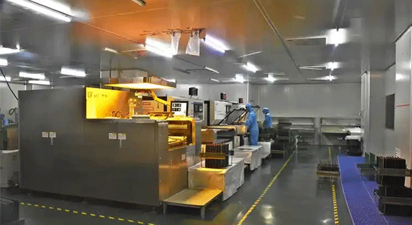
Wet Chemical Etching Process: Working Principles, Benefits & Industrial Applications
Wet chemical etching is a precision material removal process that achieves selective patterning or stripping through controlled chemical reactions between liquid etchant solutions and target material layers. Different from dry etching that relies on plasma physical bombardment, wet etching performs material dissolution entirely in a liquid phase environment at mild temperatures, delivering inherent advantages of high selectivity, zero plasma damage and high batch processing efficiency. As one of the foundational core processes in micro-nano manufacturing, it runs through the whole industrial chain from front-end wafer fabrication to back-end advanced packaging, optoelectronic device production and MEMS manufacturing. With the continuous expansion of advanced packaging and third-generation semiconductor industries, wet chemical etching, with its unique technical advantages, still plays an irreplaceable role in scenarios pursuing high surface quality and low processing damage.
I. Core Characteristics of Wet Chemical Etching Process
The liquid-phase chemical reaction mechanism endows wet chemical etching with a set of unique technical attributes different from dry etching processes. These inherent characteristics directly determine its applicable scenarios, processing quality and comprehensive economic benefits.
1. Isotropic Etching with Uniform Edge Morphology
Wet chemical etching is a typical isotropic process: the etchant reacts uniformly in all directions of the exposed material surface, forming a natural rounded undercut edge while etching vertically. This feature makes it excellent at surface smoothing, residual layer stripping and edge deburring, and the etched sidewall is smooth without sharp steps. Although it is not the first choice for high-aspect-ratio structures, its isotropic property can effectively eliminate sharp edge stress concentration and improve the long-term reliability of devices.
2. Ultra-High Material Etching Selectivity
By adjusting the composition, concentration and pH value of the etchant formula, extremely high etching selectivity can be achieved. The etch rate for the target material can be dozens or even hundreds of times that for the mask layer and the underlying substrate. It will not cause over-etching damage to the lower functional layer while removing the target layer, which is particularly critical for multi-layer stacked device structures, effectively protecting the electrical performance of core devices and reducing process defect rate.
3. Damage-Free Cold Processing Without Plasma Impact
The whole wet etching process is carried out at room temperature or mild constant temperature, with no high-energy plasma bombardment, no charge accumulation effect and no lattice damage layer on the material surface. It will not introduce residual stress, surface defects and performance degradation caused by dry etching. For sensitive devices such as optoelectronic chips and high-frequency RF devices, this zero-damage processing feature directly guarantees the working performance and service life of products.
4. High-Efficiency Batch Processing Capability
Wet chemical etching supports simultaneous processing of multiple workpieces in the same etching tank. For standard wafer production lines, it can process dozens of wafers at a time, with far higher unit time output than single-wafer dry etching equipment. This batch processing feature significantly improves production capacity, reduces single-piece processing costs, and is very suitable for large-scale mass production scenarios with mature process solutions.
5. Smooth Etched Surface with Low Roughness
Material is removed uniformly at the molecular level through chemical dissolution, and the etched surface has extremely low roughness and no recast layer, burrs or micro-cracks common in mechanical and dry etching. For optical devices and high-frequency transmission structures, the smooth surface can reduce optical loss and signal attenuation, and the excellent surface quality also eliminates the need for secondary polishing and reduces post-processing procedures.
6. Wide Compatibility Across Material Systems
Wet chemical etching covers almost all common materials in micro-nano manufacturing: different etchant systems can be used for silicon, silicon oxide, silicon nitride, gallium arsenide, and various metals such as copper, aluminum, titanium and gold. Targeted formulas are developed for different materials to ensure stable etch rate and surface quality, adapting to the diversified material requirements of different industries.
7. Cost-Effective & Easy Process Scaling
Compared with expensive dry etching equipment, wet etching equipment has a simpler structure, lower procurement and operation and maintenance costs, and easier capacity expansion. The etchant can be recycled through component adjustment and filtration, which further reduces consumable costs. For mature mass production links, wet chemical etching has obvious comprehensive cost advantages and can effectively reduce the total manufacturing cost of products.
II. Core Functions & Industrial Value
As a foundational micro-nano processing technology, wet chemical etching undertakes six core functional values in the industrial chain, solving multiple process pain points and creating tangible economic benefits for downstream industries.
1. Selective Thin Film Patterning & Stripping
The most core function is to realize selective removal and pattern transfer of thin film layers. With the protection of photoresist or hard mask, the target material area exposed by the mask is accurately dissolved, and the pattern defined by photolithography is transferred to the functional film layer. It is also widely used in the stripping of residual layers and the removal of surface sacrificial layers, which is an essential process link in the device manufacturing process.
2. Wafer Surface Smoothing & Defect Repair
Wet etching can uniformly remove a thin layer of material on the wafer surface, eliminate surface micro-scratches, lattice damage and processing defects left by the previous process, and realize surface smoothing and defect repair. This function can significantly improve the surface quality of wafers, reduce device leakage and failure risks, and lay a foundation for subsequent high-quality film deposition.
3. Support for Large-Scale Mass Production
The efficient batch processing capability of wet etching provides strong support for large-scale mass production of semiconductors, photovoltaics and other industries. It can stably output high-yield finished products under the premise of ensuring quality, help enterprises shorten production cycles, improve overall production line efficiency, and meet the market demand for large-scale supply of mature products.
4. Low-Damage Processing for High-Sensitivity Devices
For optoelectronic devices, RF chips and MEMS structures that are sensitive to plasma damage and stress, wet etching provides a low-damage processing scheme. It will not cause device performance degradation caused by charge injection and lattice damage, effectively improve product yield and long-term reliability, and support the performance iteration of high-end sensitive devices.
5. Process Compatibility with Standard Production Lines
Wet chemical etching has high process compatibility and can be seamlessly connected with standard processes such as photolithography, cleaning and film deposition. It can be integrated into the existing production line without large-scale transformation, and can be used in conjunction with dry etching to form a composite process scheme, giving full play to the advantages of different processes.
6. Optimization of Total Manufacturing Cost
With low equipment investment, low consumable cost and high processing efficiency, wet chemical etching can significantly reduce the unit processing cost for mass production links. For cost-sensitive industries such as photovoltaics and PCB, it effectively reduces the production threshold while ensuring quality, and improves the market competitiveness of end products.
III. Main Industrial Application Fields
Thanks to its unique technical advantages, wet chemical etching has been widely used in many high-end manufacturing fields.
1. Semiconductor Wafer Front-End Manufacturing
This is the most core application field of wet chemical etching. It is used for pattern etching of oxide layers, nitride layers and metal layers in front-end wafer processing, as well as wafer surface cleaning, photoresist stripping and defect repair. It cooperates with dry etching to complete the fabrication of transistor structures and interconnection lines, and is one of the essential basic processes in wafer manufacturing.
2. Advanced Semiconductor Packaging
In advanced packaging scenarios such as fan-out packaging and 2.5D/3D packaging, wet etching is used for the fabrication of redistribution layers, under bump metallization and metal shielding layers. Its stress-free and burr-free processing characteristics are very suitable for ultra-thin packaging substrates, ensuring the electrical performance and reliability of high-density packaging structures, and supporting the development of advanced packaging towards thinner and higher density.
3. MEMS & Micro-Nano Device Manufacturing
Wet etching is widely used in the structural release and micro-structure fabrication of MEMS sensors, microfluidic chips and micro-optical devices. It can realize the release of suspended structures without mechanical damage, and process micro-channels and cavity structures with smooth surfaces. The isotropic etching feature can also realize special three-dimensional structures such as V-grooves and hemispherical cavities, which cannot be easily achieved by dry etching.
4. Photovoltaic Solar Cell Production
In the photovoltaic industry, wet chemical etching is used for surface texturing, edge isolation and emitter etching of solar cells. The textured light-trapping structure prepared by etching can significantly improve the light absorption efficiency of cells and increase photoelectric conversion rate. Its high-efficiency batch processing capacity perfectly matches the large-scale production characteristics of the photovoltaic industry and effectively controls production costs.
5. PCB & FPC Fine Circuit Fabrication
For high-density printed circuit boards and flexible circuit boards, wet chemical etching is the core process for fine circuit patterning. It can accurately fabricate micron-level circuit lines on copper-clad substrates, with smooth line edges and no burrs, ensuring stable signal transmission. It supports the production of high-density, multi-layer circuit boards and meets the miniaturization demand of electronic products.
6. Optical & Optoelectronic Component Processing
In the fields of optical communication, laser devices and display components, wet etching is used to fabricate micro-lens arrays, optical gratings, waveguide structures and light-emitting diode mesa structures. The ultra-smooth etched surface reduces optical loss, ensures the optical performance of devices, and provides reliable processing support for the optoelectronic industry.
7. Medical Microfluidic & Biochip Manufacturing
Medical microfluidic chips, biosensors and lab-on-a-chip devices use wet etching to fabricate micro-channel, micro-cavity and micro-electrode structures. The smooth surface without burrs is easy to clean and sterilize, and the biocompatible material processing meets medical safety requirements, supporting the innovation and development of in-vitro diagnosis and precision medical devices.
Conclusion
In summary, wet chemical etching, with its core advantages of high selectivity, zero plasma damage, smooth surface and efficient batch processing, occupies an irreplaceable position in micro-nano manufacturing. It complements dry etching technology, and together they build a complete precision etching process system, supporting the development of semiconductors, optoelectronics, MEMS, photovoltaics and other industries.
With the rapid development of advanced packaging, third-generation semiconductors and microfluidic medical devices, the market demand for high-quality, low-damage wet etching processes will continue to grow. In the future, wet chemical etching technology will continue to evolve towards higher precision, more environmentally friendly formulas and more intelligent process control, further expanding its application scope and providing more solid technical support for the innovation and upgrading of high-end manufacturing industries.