Chemical Photo Etching: Process, Characteristics, Functions & Industrial Applications
Chemical photo etching, commonly referred to as photochemical etching (PCM) or metal photo etching, is an advanced non-contact cold subtractive manufacturing technology that combines high-precision photolithography patterning with controlled chemical dissolution. Unlike conventional fabrication methods such as stamping, laser cutting and CNC milling that rely on mechanical force or high-energy thermal impact to remove material, photo etching shapes precision metal parts through uniform molecular-level chemical reaction at room temperature, delivering exceptional accuracy, edge quality and material integrity.
Over the past decade, as global high-end manufacturing continues to push toward component miniaturization, higher reliability and faster product iteration, chemical photo etching has evolved from a niche processing technique into a mainstream precision fabrication solution. It effectively addresses long-standing pain points of traditional processes, including part deformation, burr formation, high tooling costs and limited design freedom for complex thin-walled parts. Today, the technology serves as a foundational manufacturing process across a wide range of high-tech sectors, enabling product innovations that would be economically or technically unfeasible with older methods.
I. Core Characteristics of Chemical Photo Etching
The unique combination of photolithographic pattern transfer and room-temperature chemical corrosion gives chemical photo etching a set of core advantages that traditional manufacturing technologies cannot match. These characteristics run through the entire production cycle from prototyping to mass production, directly determining the performance, reliability and total cost of finished metal parts.
1. Micron-Level Pattern Fidelity & Ultra-High Dimensional Accuracy
The photolithography-based patterning system achieves extremely high pattern transfer fidelity, transferring digital CAD designs onto metal substrates with near-zero distortion. Standard production dimensional tolerance stably reaches ±0.005mm to ±0.01mm, with minimum achievable feature line width down to 0.02mm. For double-sided etching, front-to-back alignment accuracy can be controlled within ±0.002mm, enabling precise production of complex multi-layer composite structures.
Unlike laser cutting, which accumulates positioning errors across large arrays of features, or stamping, which suffers from die wear and springback deviation, photo etching forms all features simultaneously through uniform chemical reaction. Every hole, slot and contour on the entire sheet etches at the exact same rate, delivering consistent dimensions across the full production sheet with zero cumulative error. This level of precision is irreplaceable for high-density components such as encoder gratings, micro-filter arrays and fine-pitch connectors.
2. Completely Burr-Free & Smooth Edge Profile
Chemical photo etching removes metal through uniform atomic-level dissolution, producing smooth, vertically rounded edges that are completely free of burrs, flanging, tool marks and sharp protrusions. There is no need for secondary deburring, polishing or finishing operations, which not only reduces production steps and costs, but also avoids dimensional damage and surface defects caused by post-processing of thin precision parts.
By contrast, stamping, punching and CNC machining inevitably produce burrs along cut edges. Sharp burrs can scratch mating surfaces, accelerate wear, shed micro-debris and contaminate sensitive systems such as semiconductors and medical devices. The burr-free nature of photo etching eliminates all these risks, making it a mandatory process for high-cleanliness, high-safety application scenarios.
3. Stress-Free Cold Processing & Full Material Property Retention
As a room-temperature cold processing technology, chemical photo etching applies no mechanical extrusion force, punching impact or high-temperature thermal load to the metal substrate. It introduces zero residual internal stress, zero lattice deformation and zero heat-affected zone (HAZ), preserving 100% of the base material’s native mechanical, electrical, thermal and corrosion-resistant properties.
Stamped parts typically carry large residual stresses that gradually release during temperature cycling and long-term service, causing dimensional drift and fatigue fracture. Laser-cut parts have a 0.1–0.3mm heat-affected zone that destroys the passive film of stainless steel and reduces corrosion resistance, and alters the elastic properties of spring materials. Photo-etched parts suffer from none of these degradation effects, maintaining stable performance throughout their entire service life.
4. Unlimited Design Freedom & Zero Complexity Premium
Chemical photo etching imposes no cost penalty for geometric complexity. Intricate curves, multi-track composite patterns, dense micro-hole arrays, fine spring fingers and irregular custom contours all cost the same to produce as simple basic shapes. Every feature etches simultaneously in a single processing pass, so design complexity does not increase cycle time, labor cost or material waste.
This gives product engineers complete freedom to optimize part performance based on functional requirements, without being constrained by manufacturing limitations. Designs optimized through optical simulation, fluid dynamics simulation or mechanical finite element analysis can be reproduced 1:1 directly, enabling higher-performance part designs that were previously impossible or prohibitively expensive to manufacture.
5. Low-Cost Rapid Tooling & Fast Prototyping
Instead of expensive hardened steel stamping dies that cost thousands of dollars and require weeks of machining, chemical photo etching uses digital photomask films as tooling. A single photomask costs less than 1/50 of a typical stamping die and can be produced in just a few hours. Design modifications only require updating the CAD file and plotting a new mask, with no rework costs or long lead times.
Prototype samples can typically be delivered within 24–48 hours after drawing confirmation, dramatically shortening product R&D cycles and reducing trial-and-error costs. The process supports order quantities from single-digit prototype samples to millions of mass-produced parts, with no minimum order threshold, making it ideal for today’s multi-variety, small-batch customized manufacturing model.
6. Exceptional Batch-to-Batch Consistency
Chemical photo etching production relies on digital pattern transfer and closed-loop controlled chemical reaction systems. Automated production lines maintain precise, constant control over etchant concentration, temperature, spray pressure and conveyor speed, ensuring that every part on every sheet has identical dimensions, shape and performance.
Unlike stamping, which suffers from gradual die wear and quality drift over long production runs, photo etching maintains completely consistent accuracy from the very first part to the millionth part. Comprehensive yield remains stable above 98.5%, with no hidden costs for tool maintenance, repair or replacement. This high repeatability is highly valued by automotive, medical and aerospace customers with strict long-term quality and traceability requirements.
7. High Cleanliness & Regulatory Compliance
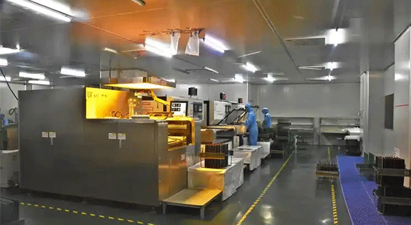
All photo etching production takes place in temperature-controlled clean workshops. Finished parts go through multiple stages of deionized water ultrasonic cleaning and vacuum drying, leaving no oil residue, photoresist residue, metal debris or chemical contaminants on the surface, reaching electronic-grade and medical-grade cleanliness levels.
The smooth, burr-free, non-porous surface also resists bacterial growth and dirt accumulation, making parts easy to clean and sterilize. Etched components can meet FDA, LFGB and ISO 10993 biocompatibility standards, supporting compliance for food contact and medical device applications.
II. Core Functions & Value of Chemical Photo Etched Components
Beyond simply shaping metal parts, chemical photo etching delivers six core functional values that solve long-standing pain points in precision manufacturing and create tangible economic benefits for downstream customers.
1. Integration of Multi-Functional Patterns in a Single Part
The most fundamental value of photo etching is its ability to integrate multiple functional features — conductive circuits, fluid filter holes, elastic beams, sensing gratings and mounting holes — into a single thin metal sheet in one processing step. This eliminates the need to assemble multiple separate components, reduces overall product volume, improves structural reliability and lowers total system cost.
For example, a single etched encoder disc integrates optical grating tracks, a central mounting hole, positioning notches and a zero-index mark all at once, replacing an assembly of three to four separate parts. This integration capability is a key enabler of ongoing miniaturization in electronics and medical devices.
2. Precision Dimensional Control for High-Accuracy Assembly
Micron-level forming accuracy and stress-free dimensional stability allow etched parts to achieve extremely tight assembly fits with mating components. They compensate for manufacturing tolerances of other parts, reduce tolerance stack-up and improve the overall assembly accuracy and operational stability of finished equipment.
For precision instruments, optical systems and semiconductor manufacturing equipment, stable dimensional accuracy directly determines the working accuracy and repeatability of the entire machine. Photo-etched shims, spacers and positioning reference parts provide a reliable dimensional benchmark for high-precision assembly.
3. Enhanced Reliability & Extended Service Life
By preserving complete material properties and eliminating internal defects such as residual stress and micro-cracks, chemical photo etching greatly improves the long-term reliability and fatigue life of parts. There are no stress concentration points or burr edges to act as fatigue crack initiation sites, so parts can withstand millions of cycles of loading, vibration and temperature change without failure.
For mission-critical products in aerospace, medical and industrial automation fields, this improved reliability directly reduces equipment failure rates, cuts maintenance costs and extends overall service life. In many applications, etched parts deliver 3 to 5 times the service life of stamped or laser-cut equivalents.
4. Accelerated R&D and Product Innovation
Low tooling cost and fast prototyping allow companies to test multiple design iterations quickly and inexpensively. Engineering teams can evaluate 3 to 5 different design variants in the time it would take to produce a single stamping die, dramatically speeding up new product development and reducing R&D investment risk.
This speed-to-market advantage is particularly valuable in fast-moving industries such as consumer electronics and new energy, where being first to market with an optimized design can capture significant market share. Companies can also respond more quickly to changing customer requirements and emerging market opportunities.
5. Seamless Scalability from Prototype to Mass Volume
The exact same chemical photo etching process used to produce 10 prototype samples also produces millions of production parts with identical quality and performance. There is no need to re-engineer the part, re-qualify the process or switch to a different manufacturing method when scaling from development to full production.
This seamless scalability ensures consistent part performance from early prototyping through full mass production, eliminates the cost and risk of process transfer, and avoids costly design rework caused by differences between prototype and production processes.
6. Support for Strict Industry Regulatory Compliance
The inherent cleanliness, material integrity and consistent quality of photo-etched parts help customers meet stringent industry regulatory requirements. For medical devices, automotive components and aerospace hardware, which require extensive documentation and qualification, the traceable, repeatable nature of the process simplifies certification and reduces compliance risk.
III. Major Industrial Applications of Chemical Photo Etching
Thanks to its unique combination of precision, flexibility and material compatibility, chemical photo etching is used across a wide range of high-tech and industrial sectors, with new application areas emerging continuously as manufacturing technology advances.
1. Electronics & Semiconductor Manufacturing
This is the largest and most mature application field for chemical photo etching. Common etched components include semiconductor lead frames, EMI shielding cans, heat pipe and vapor chamber wick structures, connector spring contacts, ceramic package lids and flexible circuit substrates. The process’s micron-level precision, burr-free quality and stress-free structure perfectly support the ongoing trend toward smaller, denser and more reliable electronic components.
2. Aerospace & Defense Aviation
Aerospace customers use photo-etched precision shims, hydraulic filter screens, sensor components, heat dissipation parts and elastic contacts in aircraft, satellites and missile systems. Full material property retention, stress-free stability and high fatigue reliability meet the extreme reliability demands of aerospace applications, where failure is unacceptable. Parts must withstand extreme temperatures, intense vibration and corrosive environments over decades of service.
3. Medical Devices & Life Sciences
Medical-grade etched components include surgical instrument parts, implantable electrodes, infusion filter meshes, biosensor chips and orthodontic brackets. Burr-free surfaces, biocompatibility and resistance to autoclave sterilization comply with strict medical safety standards. The technology supports advanced medical applications from minimally invasive surgical instruments to in-vitro diagnostic devices.
4. Automotive & New Energy Vehicles
In the automotive sector, chemical photo etching produces encoder discs for drive motors, transmission filter screens, battery current collectors, hydrogen fuel cell bipolar plates and connector springs. High batch consistency, corrosion resistance and long-term durability satisfy strict automotive quality requirements, and the technology is growing rapidly alongside the global expansion of electric and hydrogen fuel cell vehicles.
5. Industrial Automation & Motion Control
Etched encoder discs, precision shims, flat springs and hydraulic filter screens are foundational components in servo motors, CNC machine tools, industrial robots and automated production lines. They deliver the stable, high-accuracy position feedback and reliable fluid control required for modern smart manufacturing, ensuring consistent production quality and equipment uptime.
6. Consumer Electronics & Wearable Devices
Smartphones, wireless earbuds, camera modules and wearable devices incorporate large numbers of photo-etched parts: speaker dust meshes, VCM camera springs, SIM contact springs, button domes and decorative trim. Ultra-thin forming capability, complex pattern freedom and high-volume consistency match the consumer electronics industry’s requirements for slim design, rapid product iteration and stable mass supply.
7. Energy & Environmental Engineering
In the new energy and environmental protection sectors, photo etching is used to manufacture fuel cell bipolar plates, electrolyzer electrodes, industrial filter elements and water treatment components. Excellent corrosion resistance and precise flow channel geometry improve energy conversion efficiency and extend equipment service life in demanding operating environments, supporting the global transition to clean energy.
Conclusion
Chemical photo etching combines the pattern precision of photolithography with the uniform material removal of chemical corrosion, creating a manufacturing process that delivers burr-free, stress-free, micron-accurate metal parts without mechanical force or thermal damage. What begins as a digital CAD design passes through coating, exposure, development, etching and stripping to emerge as a fully finished precision component in a single, highly repeatable production flow.
As global manufacturing continues to advance toward higher precision, miniaturization and faster innovation, chemical photo etching is growing in importance across nearly every high-tech industry. Its unique ability to deliver complex, high-precision parts quickly, reliably and cost-effectively makes it a key enabling technology for the next generation of electronics, medical devices, aerospace systems and clean energy equipment. Looking ahead, the technology will continue evolving toward even higher resolution, wider material compatibility and more intelligent production, further expanding its application scope and value in advanced manufacturing.