
How Does Chemical Etching Work? Step-by-Step Process & Industrial Applications
Chemical etching, also widely referred to as photochemical etching (PCM) or photo etching, is an advanced non-contact cold subtractive manufacturing technology that produces highly precise metal components through controlled chemical dissolution. Unlike traditional stamping, laser cutting and CNC milling that rely on mechanical force or high-energy thermal impact to remove material, chemical etching shapes parts at the molecular level via uniform chemical reaction at room temperature. For engineers and product designers working on miniaturized, high-precision metal parts, understanding how chemical etching works is critical for selecting the optimal fabrication process and unlocking design possibilities that traditional methods cannot achieve.
As global manufacturing continues to push toward higher precision, lighter weight and faster product iteration, chemical etching has become an indispensable process in high-end sectors such as electronics, aerospace, medical devices and new energy. This article explains the working principle of chemical etching in full detail, walks through every step of the production flow, analyzes its core technical characteristics and functional advantages, and introduces its major industrial applications.
I. Working Principle of Chemical Etching
At its core, chemical etching works by selectively protecting areas of a metal sheet with a photoresist mask, then immersing the sheet in a controlled chemical etchant solution that dissolves the unprotected metal areas at a predictable, uniform rate. The process follows two foundational principles: selective masking and isotropic chemical corrosion.
First, the target part geometry is transferred from a digital CAD file onto a high-precision photomask film. The photomask is then used like a photographic negative during UV exposure: UV light passes through the transparent areas of the mask and cures the photoresist coating on the metal surface, forming a tough, acid-resistant protective layer. The unexposed photoresist remains soluble and is washed away during development, exposing the bare metal underneath.
In the subsequent etching step, the prepared metal sheet is sprayed or immersed with heated etchant solution. The etchant chemically reacts with the exposed bare metal, dissolving it uniformly from both sides until the desired geometry is fully cut through. The cured photoresist protects the masked areas from corrosion, preserving the exact shape of the final part. After etching, the remaining photoresist is stripped away, leaving the finished precision metal component.
Because the reaction occurs uniformly across all exposed metal surfaces simultaneously, all features on the sheet form at the same rate with identical dimensional accuracy. There is no mechanical contact, no shear force and no heat input, so the material retains its original mechanical, chemical and physical properties completely.
II. Step-by-Step Chemical Etching Process
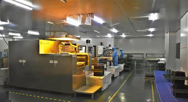
A complete chemical etching production line consists of eight sequential process stages. Each step is tightly controlled for temperature, concentration, time and cleanliness to ensure consistent, repeatable high-precision results.
1. Material Preparation & Pre-Treatment
The process begins with selecting the appropriate metal sheet material and thickness according to part requirements. Common materials include stainless steel, copper, beryllium copper, titanium, nickel alloy and aluminum. Sheets are cut to standard production sizes, then go through a multi-stage degreasing and surface preparation line.
Surface pre-treatment is critical for ensuring strong photoresist adhesion. The metal sheet passes through alkaline cleaning, acid pickling, micro-etching roughening and pure water rinsing to remove rolling oil, oxide layers and surface contaminants, creating a uniformly clean, slightly textured surface. Poor pre-treatment leads to photoresist peeling or undercutting during etching, which directly reduces part accuracy and yield.
2. Photoresist Coating & Drying
Next, a uniform layer of UV-sensitive dry film photoresist is laminated onto both sides of the metal sheet under controlled temperature and pressure, or applied via liquid coating for ultra-thin foils. The coated sheet then passes through a low-temperature drying oven to evaporate solvent and solidify the photoresist into a smooth, uniform, light-sensitive film.
Coating thickness is precisely controlled based on material thickness and feature resolution. For high-resolution parts with features below 0.05mm, a thinner photoresist is used for sharper pattern definition; for thicker materials requiring longer etching time, a thicker, more durable photoresist is applied to withstand longer exposure to etchant.
3. UV Exposure & Pattern Transfer
The dried photoresist-coated sheet is aligned between two matching photomask films on a precision UV exposure machine. High-intensity ultraviolet light is projected through the mask, curing the photoresist in all transparent areas of the mask. The opaque areas block UV light, leaving the photoresist underneath uncured.
Modern exposure machines achieve alignment accuracy of ±0.002mm, ensuring front-to-back pattern alignment for double-sided etching. This step is where the digital CAD design is physically transferred onto the metal sheet with micron-level fidelity. The photomask itself is plotted directly from CAD files, so design changes only require producing a new mask film at very low cost.
4. Development & Pattern Reveal
After exposure, the sheet moves into the developer station. A mild alkaline developer solution is sprayed onto the surface, dissolving and washing away the uncured photoresist while leaving the cured, hardened photoresist firmly attached.
After development, the exact part pattern is revealed on the metal surface: areas covered by cured photoresist will remain as the final part, and all exposed bare metal will be etched away. At this stage, a first-piece inspection is performed to verify pattern dimensions, alignment accuracy and photoresist quality before the sheet proceeds to etching.
5. Precision Etching & Material Removal
Etching is the core material-removal step of the whole process. The developed sheet is fed into a horizontal conveyorized etching machine, where heated etchant solution is uniformly sprayed onto both sides of the sheet from arrays of precision nozzles.
For most common metals like stainless steel, ferric chloride solution is used as the etchant. The solution concentration, temperature, spray pressure and conveyor speed are all tightly controlled to maintain a constant, predictable etch rate. The etchant reacts chemically with the exposed metal, dissolving it into metal salts that are carried away by the flowing solution. Etching proceeds vertically downward and also slightly sideways under the edge of the photoresist — a natural effect called undercut. Experienced etchers compensate for undercut in the original photomask design so that final part dimensions match the CAD specification exactly.
6. Photoresist Stripping
Once etching is complete, the sheet exits the etching chamber and immediately goes through rinse stages to stop the reaction and remove residual etchant. It then enters the stripping station, where a strong alkaline stripping solution removes all remaining cured photoresist from the part surfaces.
After stripping, the bare finished metal parts remain attached to the remaining sheet frame by small support tabs. The parts are clean, burr-free and fully formed, with all original material properties intact. No secondary deburring or finishing is required for most applications.
7. Cleaning & Drying
Stripped parts go through multiple stages of DI (deionized) water ultrasonic cleaning to remove all traces of chemistry and particulate contamination, then pass through a hot air or vacuum drying system. The result is clean, dry, contamination-free metal components ready for inspection or additional secondary operations.
For medical, semiconductor and aerospace grade parts, class 1000 cleanroom processing and additional passivation treatments are available to meet ultra-high cleanliness and corrosion resistance requirements.
8. Dimensional Inspection & Quality Control
The final step is full quality inspection. Each production batch undergoes dimensional verification using vision measuring systems, micrometers and optical comparators to confirm tolerance compliance, flatness, edge quality and surface finish. Additional tests such as salt spray, hardness and cleanliness testing can be performed according to customer specifications.
Approved parts are then packaged according to application requirements — typically with anti-tarnish paper and ESD packaging for electronic and medical components — and prepared for shipment.
III. Key Characteristics of the Chemical Etching Process
The unique chemical forming mechanism gives chemical etching a set of core advantages that traditional manufacturing technologies cannot match. These characteristics directly determine the performance, cost and delivery advantages of etched parts.
1. Completely Burr-Free & Stress-Free Forming
Because metal is removed by uniform dissolution rather than mechanical shearing or melting, etched parts have perfectly smooth, rounded, burr-free edges with no sharp protrusions, flanging or micro-cracks. There is zero residual stress introduced into the material, and no heat-affected zone that would alter material properties. This is the single most important differentiator from stamping and laser cutting, and it makes etching indispensable for high-reliability, high-cleanliness applications.
2. Micron-Level Dimensional Accuracy
Standard production tolerance for chemical etching is ±0.005mm to ±0.01mm, with minimum feature size down to approximately 1.1 times material thickness. All features across the entire sheet etch at the same rate, so dimensional consistency is extremely high — there is no tool wear drift over time as with stamping, and no positioning error accumulation as with laser cutting. This level of precision is essential for components like encoder discs, filter screens and precision springs.
3. Unlimited Geometry Complexity
Chemical etching imposes no cost penalty for complex geometries. Intricate curves, multi-track patterns, micro-hole arrays, fine spring fingers and irregular contours all cost the same to produce as simple circles. Every feature etches simultaneously in a single pass, so complexity does not increase cycle time or price. This gives designers complete freedom to optimize part performance without being constrained by manufacturing limitations.
4. Full Material Property Retention
As a room-temperature cold process with no mechanical force, etching preserves 100% of the base material’s native mechanical, electrical, thermal and corrosion properties. There is no work hardening, no thermal softening and no damage to surface passivity layers. For spring parts, this means consistent force values and long fatigue life; for stainless steel parts, this means full corrosion resistance with no weakened edge areas.
5. Low-Cost Rapid Tooling & Prototyping
Instead of expensive steel stamping dies that cost thousands of dollars and take weeks to produce, chemical etching uses digital photomask films that cost a tiny fraction and can be produced in hours. Design changes only require a new mask file, with no rework costs. Prototype samples can typically be shipped within 24–48 hours, enabling extremely fast design iteration and dramatically reducing new product development time and risk.
6. Excellent Batch-to-Batch Consistency
Because the process is digitally controlled and chemically uniform, quality remains identical from the first part to the millionth part. There is no tool wear to cause gradual dimensional drift, and automated closed-loop process control ensures consistent etch rate across every production run. This high repeatability is highly valued by automotive, medical and aerospace customers with strict long-term quality requirements.
7. Broad Material Compatibility
Chemical etching works with virtually all common engineering metals: 304/316L stainless steel, beryllium copper, phosphor bronze, pure copper, titanium, nickel silver, Invar, Hastelloy, Monel, molybdenum and more. Each material uses a tailored etchant formulation optimized for uniform etch rate and high surface quality. Even materials that are difficult to stamp or laser cut, such as brittle alloys and highly reflective copper, etch reliably with excellent results.
IV. Core Functions & Value of Chemical Etching
Beyond simply shaping metal parts, chemical etching delivers six core functional values that solve long-standing pain points in precision manufacturing.
1. Integration of Complex Functional Patterns
Etching enables multiple functional features — electrical circuits, fluid channels, elastic beams, grating patterns and mounting holes — to be integrated into a single thin metal sheet in one process step. This eliminates assembly of multiple separate parts, reduces overall product size, improves reliability and lowers total system cost.
2. High-Precision Dimensional Control for Precision Assembly
Micron-level accuracy and stress-free dimensional stability allow etched parts to fit together with extremely tight assembly tolerances. This improves overall equipment alignment accuracy, reduces backlash and play, and enables higher performance in precision machinery, optical systems and semiconductor equipment.
3. Clean, Damage-Free Parts for High-Sensitivity Applications
The burr-free, particle-free, stress-free nature of etched parts eliminates contamination and fatigue failure risks. This makes the process suitable for the most sensitive applications including medical implants, semiconductor processing equipment and aerospace flight hardware where reliability and cleanliness are non-negotiable.
4. Accelerated Product Development & Innovation
Low tooling cost and fast prototyping allow companies to test multiple design iterations quickly and inexpensively. This speeds up new product launch, reduces R&D investment risk and enables manufacturers to respond faster to changing market demands — a major competitive advantage in fast-moving industries like consumer electronics.
5. Scalable Production from Prototype to Mass Volume
The same process that produces 10 prototype samples also produces millions of production parts with identical quality. There is no need to re-engineer the part or switch manufacturing methods when scaling from development to full production, ensuring consistent performance and avoiding costly re-qualification.
6. Cost-Effective High-Volume Precision Manufacturing
For medium and high volume production of complex thin metal parts, chemical etching often delivers lower total cost than stamping, laser or CNC machining. There are no expensive dies to amortize, no secondary deburring operations, higher material utilization and higher overall yield.
V. Major Industrial Applications of Chemical Etching
Thanks to its unique combination of precision, flexibility and material compatibility, chemical etching is used across a wide range of high-tech and industrial sectors.
1. Electronics & Semiconductor Industry
This is the largest application area. Etched parts include semiconductor lead frames, EMI shielding cans, heat pipe wick structures, connector spring contacts, lead frames and ceramic package lids. The process’s high precision, burr-free quality and stress-free structure support the ongoing trend toward smaller, denser and more reliable electronic components.
2. Aerospace & Defense
Aerospace customers use etched precision shims, filter screens, sensor components, heat dissipation parts and elastic contacts for aircraft, satellites and missile systems. Full material property retention, stress-free stability and high fatigue reliability meet the extreme reliability demands of aerospace applications, where failure is not an option.
3. Medical Devices & Life Sciences
Medical-grade etched components include surgical instrument parts, implantable electrodes, infusion filter meshes, biosensor chips and orthodontic brackets. Burr-free surfaces, biocompatibility and sterilization resistance comply with strict medical safety standards and support advanced medical technologies from minimally invasive surgery to diagnostic devices.
4. Automotive & New Energy
In the automotive sector, etching produces encoder discs, transmission filter screens, battery current collectors, fuel cell bipolar plates and connector springs. High batch consistency, corrosion resistance and long-term durability satisfy strict automotive quality requirements and support the rapid growth of electric and hydrogen fuel cell vehicles.
5. Industrial Automation & Motion Control
Etched encoder discs, precision shims, flat springs and hydraulic filter screens are foundational components in servo motors, CNC machine tools, industrial robots and automated production lines. They deliver the stable, high-accuracy position feedback and reliable fluid control required for modern smart manufacturing.
6. Consumer Electronics & Wearables
Smartphones, earbuds, cameras and wearables incorporate large numbers of etched parts: speaker dust meshes, VCM camera springs, SIM contact springs, button domes and decorative trim. Ultra-thin forming capability, complex pattern freedom and high-volume consistency match the consumer electronics industry’s requirements for slim design, fast iteration and mass production.
7. Energy & Environmental Engineering
In new energy and environmental sectors, etching is used for fuel cell bipolar plates, electrolyzer electrodes, industrial filter elements and water treatment components. Excellent corrosion resistance and precise flow control improve energy conversion efficiency and extend equipment service life in demanding operating environments.
Conclusion
Chemical etching works by combining photolithographic pattern transfer with controlled chemical dissolution to produce burr-free, stress-free, micron-accurate metal parts without mechanical force or heat input. What begins as a digital CAD file passes through coating, exposure, development, etching and stripping to emerge as a fully finished precision component in a single, highly repeatable production flow.
As global manufacturing continues to advance toward higher precision, miniaturization and faster innovation, chemical etching is growing in importance across nearly every high-tech industry. Its unique ability to deliver complex, high-precision parts quickly, reliably and cost-effectively makes it a key enabling technology for the next generation of electronics, medical devices, aerospace systems and clean energy equipment. Understanding how the process works allows engineers and product teams to fully leverage its advantages, push design boundaries and bring better products to market faster.