
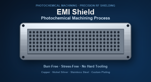
photo etching process
The EMI shield photochemical machining process is the preferred manufacturing route for precision RF shielding in modern electronics. As a core protection component that blocks electromagnetic interference, photo-etched EMI shields combine fine feature accuracy, burr-free edges and stress-free processing. Understanding the process steps helps buyers evaluate both cost and quality correctly.
The photochemical machining process consists of several steps: cleaning and coating the metal foil with photoresist, exposing the shield pattern through a phototool, developing the image, chemically etching away unwanted metal, and finally stripping the remaining resist. Raw materials mainly include copper, brass, nickel silver, stainless steel and aluminum foil, and material type plus thickness will change the base cost directly. Because the pattern is transferred optically, no expensive hard tooling is required, keeping prototypes and custom designs affordable.
Process control accounts for a large share of EMI shield cost. Etchant concentration, temperature and line speed determine edge quality and aperture accuracy; finer features and tighter tolerances demand more controlled processing. Different feature sizes and tolerance requirements will lead to obvious price differences. Part size, feature density and order quantity also affect the final unit cost. Large volume mass production can achieve significant economies of scale and cut down per-piece cost obviously.
Our factory applies the photochemical machining process to supply custom EMI shields for consumer electronics, automotive electronics, telecommunications and medical devices. We support prototype sampling, low volume trial runs and large-scale mass production. Every batch undergoes strict dimension, flatness and shielding inspection to guarantee stable electromagnetic compatibility.
When evaluating EMI shield photochemical machining cost, buyers should avoid only focusing on low unit price. Poorly controlled etching with rough edges or inconsistent apertures may reduce shielding effectiveness and raise device failure risk, lifting long-term operating expenses. It is essential to evaluate cost alongside process precision, plating quality and dimensional consistency.