
press-fit pin etching
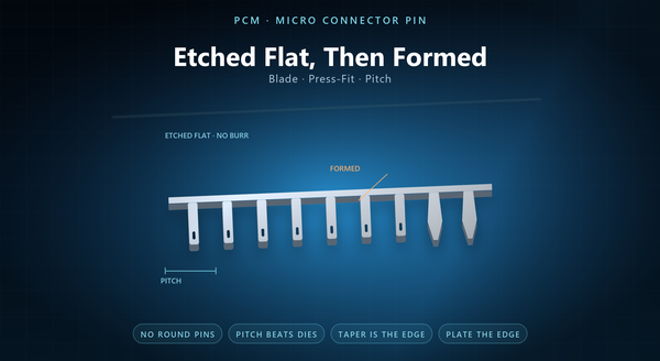
Photo chemical machining for micro connector pin starts with an admission that saves a project: etching does not make a round pin. It makes a flat blank — a blade, a spring contact, a press-fit tail, a lead — and something else makes it three-dimensional. The alternative is a flat contact or a different process, and both are worth stating at the first meeting. That is not a limitation to work around; That is not a limitation to work around; it is the reason etching reaches pitches that stamping cannot, because a flat process can hold a 0.2 mm gap while a die cannot easily punch one. A customer who asks for a 0.3 mm round pin has to be told early and told what the alternative is, and the blank is also the part that carries the tolerances, because forming adds error rather than removing it.
1. A Pin Is Not Flat, So What Is Etched
Three things are etched in a connector, and only one of them is pin-shaped.
The first is the flat blank: a strip of contacts on a carrier, each one a flat profile that will be bent, coined and plated afterwards. This is the classic etched connector part.
The second is the press-fit tail, which is a flat compliant pin with an eye or a slot; it is inserted into a plated through-hole and relies on the flat spring rather than on a round section.
The third is the lead frame around a contact array, which is a flat frame that holds the pins at pitch until assembly.
A round pin is made by heading, turning, or deep drawing. An etched part competes where the pin is flat by function, not where it is round by function.
2. Why Micro Pitch Goes to Etching
Below a certain pitch, stamping becomes a tool problem rather than a production problem.
A die needs a punch and a die opening with a physical wall thickness between them, and that wall has to survive the press force. At a fine pitch the wall becomes a sliver, and the die wears, chips or fails. Etching has no such wall: the resist defines the gap, and the etchant simply works from both sides.
The second advantage is change. A new pitch is a new artwork, not a new tool, so a connector family with several pitches can be etched from one process and a set of files.
The third is burr direction, which matters more in a connector than in most parts and is covered below. A die at a fine pitch is also expensive to make and slow to change, which matters on a connector family; etching’s penalty is the taper, and a design that ignores the taper will fight its own acceptance.
3. The Four Etched Contact Families
Four families cover most of the work, and they are worth naming because each has its own acceptance.
A blade contact is a flat tongue that slides into a socket; its critical features are the tip radius, the beam width and the contact area.
A spring contact is a cantilever that presses on a pad; its critical features are the beam length, the root radius and the free height before forming.
A press-fit tail is a flat pin with an eye; its critical features are the eye geometry, the compliant zone width and the tail length.
A lead frame is an array; its critical features are pitch, coplanarity after forming, and the tie bars that hold it until singulation. A blade’s tip radius is usually set by coining rather than by the etch and is therefore a forming tolerance, while a press-fit eye is the one etched feature where both faces must be smooth because the hole is measured.
All four are flat profiles, and all four are judged after forming, not only after etching.
4. Pitch, Web and Gauge
Three numbers are coupled, and a connector design that treats them as independent will not etch.
Pitch is the centre-to-centre distance. Web is the metal left between two adjacent contacts. Gauge is the strip thickness. The web has to be wide enough to survive being undercut from both sides, which is a function of the gauge.
The practical consequence: at a fine pitch, a thinner strip buys web. That is why micro connectors trend to thin stock, and why a design that needs a stiff pin at a fine pitch has to form the stiffness rather than buy it with thickness.
The second consequence is that the web carries the part through every handling step before forming, so a marginal web is a yield problem in the etch and an assembly problem later. A marginal web is a design that works in the lab and fails at the singulation step, and a thinner strip also reduces insertion force, which is a functional benefit rather than only a process one.
5. Burr Direction and the Mating Face
Etching has no burr, and in a connector that is a functional advantage rather than a cosmetic one.
A stamped contact carries a burr on one face, and the burr direction is set by the die. If the burr lands on the mating face, it scrapes the plating of the mating part, and a scraped contact is a contact that corrodes. Designers therefore specify which face is the burr side, and stampers control it.
An etched contact has no burr on either face, so the direction problem disappears — but a different one appears: the etched edge is a taper rather than a square edge, and the mating face is now a tapered face.
That taper is why the contact area and the wipe distance have to be specified on the etched edge rather than assumed from a square edge. A tapered edge also changes the wipe because the contact point moves as the beam deflects, so a stamped burr note is worse than useless on an etched part: it specifies a feature that does not exist.
6. Forming After the Etch
Most etched contacts are formed after etching, and the forming step is where the connector’s real tolerances come from.
Three forming operations recur. Bending puts the blade at an angle to the carrier. Coining puts a radius or a flat on the tip, which sets the contact area. And a twist or an offset puts the contact into the plane it has to mate in.
Forming is also where the etch’s advantages can be lost: a bend on a tapered edge behaves differently from a bend on a square edge, and a coined tip has to be sized against the etched edge rather than against a nominal profile.
That is why the drawing should state the forming sequence and the datum for each bend, not only the flat profile. A bend radius smaller than the strip thickness will crack a hard temper, which is an etch-plus-form decision, and a forming die is cheap compared with a punch die, which is why the hybrid route is common.
7. Plating Over an Etch Texture
A connector contact is almost always plated, and the etch surface is the substrate for that plating.
Two points matter. An etched surface is matte and slightly textured, which improves adhesion but can also trap plating solution if the rinse is incomplete; a trapped residue is a corrosion site in a humid environment.
And the plating thickness on an etched edge is not the same as on a flat face, because the edge is a taper and the current density differs. A specification that names a thickness without naming where it is measured is a specification that will disagree with the plater.
Gold over nickel is the usual finish for a contact; the nickel is the barrier and the gold is the contact surface, and both have to be continuous over the tapered edge. A plater told the location will hit it and a plater told a number will choose a location, and a gold thickness on a flat face versus a tapered edge can differ by a third.
8. Specifying and Accepting
A drawing for an etched contact should carry the alloy and temper, the gauge, the flat profile with the pitch and the web minimum, the tapered edge condition, the forming sequence with a datum per bend, the contact area after coining, and the plating with its measurement location.
Acceptance has three stages: the flat blank (profile, web, edge), the formed part (angle, coplanarity, contact area), and the plated part (thickness at a stated location, continuity, adhesion).
A drawing that separates the three stages also tells the supplier which stage to inspect. The recurring mistakes are a round pin specified to an etcher, The recurring mistakes are a round pin specified to an etcher, A first-article report for a contact should show the three stages separately. The recurring mistakes are a round pin specified to an etcher, a pitch specified without a web, a burr callout copied from a stamped drawing, a forming sequence left to the shop, and a plating thickness with no stated measurement location.