
telecommunication metal parts
Photo etching, also called photochemical machining (PCM), is a high-precision non-contact metal manufacturing process widely used to produce custom thin metal components for the telecommunication industry. Telecommunication equipment requires miniaturized, thin and stable metal parts with fine features, tight dimensional tolerance and burr-free surfaces, which photo etching can easily achieve.
A wide range of metal materials can be processed by photo etching for telecom applications, such as stainless steel, copper, nickel, brass and kovar alloy. These materials are selected for their excellent electrical conductivity, electromagnetic shielding performance, corrosion resistance and stable mechanical property to adapt to complex communication operating environments.
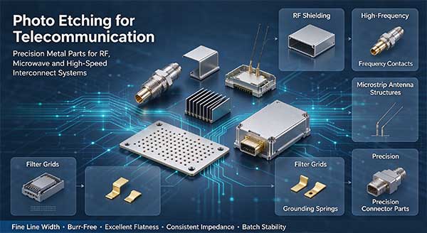
Typical photo etched telecommunication components include EMI shielding foils, precision contact shims, micro filter meshes, spring contacts, encoder discs, waveguide gaskets and locating sheets. These precision parts are essential for base stations, signal transceivers, communication modules, optical communication devices and 5G/6G communication hardware.
Unlike stamping, photo etching does not apply mechanical force to metal foils. There will be no deformation, material stress or burrs on finished parts. Complex micro patterns, tiny holes and intricate contours can be fabricated in one single process. Design modification only needs to update CAD files, greatly shortening lead time for prototype testing and mass production.
Strict quality inspection is carried out for every batch. We check flatness, aperture size, dimensional accuracy and surface quality to ensure stable signal transmission and reliable long-time operation of telecommunication devices. Our photo etching service supports fully customized sizes, thicknesses and patterns according to customer drawings for telecom projects.