
Precision Micro Chemical Etching: Process, Features & Industrial Applications
Precision micro chemical etching is an advanced high-end branch of photochemical etching technology, dedicated to fabricating ultra-fine metal components with micron-level and sub-micron level feature accuracy. Different from standard chemical etching for general industrial parts, micro etching optimizes the entire process chain from photomask resolution, photoresist coating precision to etchant uniformity control, achieving minimum feature sizes down to 15μm and dimensional tolerances within ±0.003mm. It retains all the core advantages of conventional chemical etching — burr-free forming, stress-free structure and zero complexity cost premium — while pushing precision and feature density to a new level.
Against the backdrop of global miniaturization and high integration of industrial products, conventional machining, laser processing and standard chemical etching can no longer meet the manufacturing demand of ultra-precision micro components. Precision micro chemical etching fills the gap between semiconductor lithography and general metal fabrication, providing a cost-effective mass production solution for micron-level precision metal parts. It has become an indispensable core manufacturing technology in high-end fields such as semiconductors, medical devices, optoelectronics and aerospace.
I. Core Characteristics of Precision Micro Chemical Etching
The upgraded process system endows micro chemical etching with a series of unique technical attributes that distinguish it from conventional etching processes. These characteristics define its irreplaceable position in the high-precision component manufacturing chain.
1. Sub-Micron Dimensional Accuracy & Ultra-Fine Feature Resolution
Precision micro chemical etching achieves industry-leading dimensional tolerance of ±0.003mm to ±0.005mm, with minimum machinable line width and through-hole diameter down to 15μm for ultra-thin substrates. Enabled by high-resolution chrome photomasks and double-sided precision exposure systems with ±0.001mm alignment accuracy, it delivers consistent feature dimensions across the entire production sheet, with full-surface deviation controlled within 3μm.
Unlike conventional chemical etching designed for general industrial parts, micro etching optimizes photoresist resolution, etchant spray uniformity and closed-loop process control to support ultra-dense feature arrays such as 5000+ PPR encoder gratings and 10μm-level micro filter holes. This level of precision rivals expensive semiconductor lithography processes at a fraction of the cost, making high-precision micro components accessible for a wide range of industrial applications.
2. Burr-Free & Stress-Free Ultra-Precision Forming
Consistent with all chemical-based etching processes, micro etching removes metal through uniform molecular-level dissolution, producing perfectly smooth, vertically rounded edges completely free of burrs, flanging and sharp protrusions. As a pure room-temperature cold process, it introduces zero residual internal stress, zero lattice deformation and zero heat-affected zone, fully preserving the native mechanical, electrical and chemical properties of the base material.
For ultra-thin metal foils as thin as 0.01mm, micro etching avoids the thermal warpage and mechanical deformation common in laser processing and stamping. Finished parts maintain excellent flatness of ≤0.005mm even for 0.01mm thick foils, with no curling or distortion. This damage-free forming capability is irreplaceable for fatigue-sensitive spring components and high-cleanliness medical parts.
3. Ultra-Thin Substrate Compatibility & Controlled Aspect Ratio
Precision micro etching is optimized for ultra-thin and thin substrates, supporting material thickness ranging from 0.01mm ultra-thin foil up to 0.5mm standard sheet. It delivers the best forming quality and cost performance in this thickness range, making it the preferred process for miniaturized and lightweight components.
With optimized etchant formulations and spray parameters, micro etching effectively controls lateral undercut and achieves near-vertical sidewall profiles, supporting aspect ratios up to 1.5:1 for fine features. This enables deeper, more vertical micro structures while maintaining high pattern fidelity, which is critical for micro fluid channels, deep groove arrays and other three-dimensional micro structures.
4. Ultra-High Pattern Fidelity & Zero Complexity Premium
There is no cost penalty for geometric complexity in micro chemical etching. Arbitrary curves, gradient density hole arrays, multi-track composite gratings and special-shaped micro structures all form in a single process step at the same unit cost as simple basic shapes. Complex designs optimized through optical simulation, fluid dynamics simulation or mechanical finite element analysis can be reproduced 1:1 with high fidelity.
This gives product engineers complete design freedom to optimize part performance without manufacturing constraints. For miniaturized integrated components, multiple functional features can be integrated onto a single thin metal sheet, eliminating multi-part assembly and reducing overall product size while improving reliability.
5. Electronic-Grade Cleanliness & Ultra-Low Defect Density
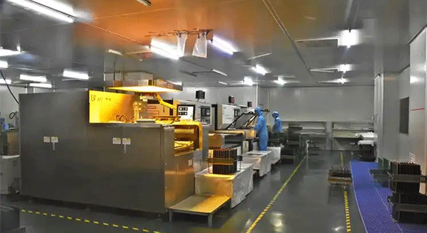
All micro etching production processes are completed in Class 1000 clean workshops, with core process steps upgraded to Class 100 environment control. Finished parts go through multi-stage ultrasonic deionized water cleaning and vacuum drying, with no oil residue, photoresist residue, metal debris or particle contaminants on the surface, reaching electronic-grade and medical-grade cleanliness.
Defect density is strictly controlled below 0.05 defects per square centimeter, far exceeding the standard of conventional industrial etching. This ultra-high cleanliness meets the strict requirements of semiconductor packaging, medical implants and optical components, avoiding product failure caused by micro particle contamination.
6. Excellent Batch Consistency & Stable Mass Production
Micro etching production relies on fully automated closed-loop control systems that maintain precise, constant control over etchant concentration, temperature, spray pressure and conveyor speed. Every part on every sheet has identical dimensions, shape and performance, with dimensional uniformity exceeding 99.8% and comprehensive yield stable above 99%.
Unlike mechanical processing which suffers from gradual tool wear and quality drift, micro etching maintains completely consistent accuracy from the very first part to the millionth part. There is no tool wear or recurring maintenance cost, and long-term batch-to-batch repeatability meets the strict quality traceability requirements of medical, aerospace and semiconductor customers.
7. Low-Cost Rapid Prototyping & Fast Design Iteration
Micro etching uses high-precision chrome photomasks as tooling, which cost far less than stamping dies and MEMS lithography masks. Design modifications only require updating the CAD file and producing a new photomask, with no expensive rework costs or long lead times.
Prototype samples can be delivered within 24–48 hours after drawing confirmation, greatly shortening the R&D cycle of new products and reducing trial-and-error costs. The process supports order quantities from single-digit laboratory samples to millions of mass-produced parts, seamlessly connecting prototype verification and large-scale mass production.
II. Core Functional Values of Precision Micro-Etched Components
As an ultra-precision manufacturing technology, micro chemical etching delivers six core functional values for downstream high-end products, providing fundamental support for product miniaturization, performance improvement and reliability enhancement.
1. Ultra-Precision Micro-Structure Integration
The most core value of micro etching is its ability to integrate multiple functional micro structures — including sensing gratings, micro filter holes, elastic beams and electrical contacts — onto a single thin metal sheet in one process step. This eliminates the need to assemble multiple separate components, reduces overall product volume, improves structural reliability and lowers total system cost.
For miniaturized devices such as medical implants and wearable sensors, integrated micro structure design can reduce component size by more than 40% while improving functional density and assembly accuracy.
2. High-Precision Sensing & Stable Signal Conversion
Micro-etched grating structures and elastic sensing elements provide high-precision signal conversion for motion and physical quantity sensors. The micron-level uniform grating lines ensure stable pulse output and high signal-to-noise ratio, supporting high-resolution position and speed detection. The stress-free elastic structure maintains consistent force value and fatigue life, ensuring long-term stable operation of sensors.
This function is the core foundation for high-precision encoders, pressure sensors and acceleration sensors, and directly determines the detection accuracy and reliability of sensing systems.
3. Micro-Filtration & Precise Flow Regulation
Micron-level uniform aperture arrays achieve accurate particle interception and precise flow control at the micro scale. The consistent pore size ensures stable filtration accuracy across the entire filter surface, and the smooth hole walls provide low and stable flow resistance, avoiding clogging and flow fluctuation caused by burrs and rough inner walls.
This function is widely used in medical infusion systems, semiconductor chemical delivery and microfluidic devices, providing reliable fluid control guarantee for precision fluid systems.
4. Miniaturized Electrical Interconnection & Electromagnetic Shielding
Micro-etched ultra-fine pitch spring contacts and miniaturized shielding structures provide reliable electrical connection and electromagnetic shielding for compact electronic devices. The high-density fine-pitch design supports more I/O channels in a smaller space, and the stress-free structure ensures stable contact force and long insertion life.
This supports the ongoing trend of miniaturization and high integration of electronic products, helping equipment manufacturers reduce product size while improving electrical performance.
5. Optical Path Control & Precise Light Modulation
Micro-etched optical slits, diaphragms and grating structures provide precise optical path control and light modulation for optoelectronic devices. The burr-free sharp edges ensure clean light cutoff without stray light and diffraction distortion, and the micron-level dimensional accuracy ensures precise control of light flux and light path position.
This function is indispensable for optical instruments, spectrometers, laser systems and imaging equipment, and directly determines the optical performance and measurement accuracy of the equipment.
6. MEMS Micro-Device Structure Fabrication
For MEMS (Micro-Electro-Mechanical Systems) devices, micro etching is used for structural layer patterning and sacrificial layer release, fabricating three-dimensional micro structures such as cantilever beams, cavities and diaphragms. High selectivity ensures that the functional structure is not damaged during the release process, and the stress-free forming improves the long-term stability of MEMS devices.
Compared with expensive semiconductor MEMS processes, micro etching provides a lower-cost mass production solution for medium-precision MEMS devices, promoting the popularization and application of MEMS technology in consumer and industrial fields.
III. Key Industrial Application Fields
Driven by the global trend of product miniaturization and high precision, precision micro chemical etching is expanding into more and more high-end industrial fields.
1. Semiconductor & Advanced Packaging
In the semiconductor industry, micro etching is used to manufacture ultra-fine pitch lead frames, miniaturized EMI shielding cans, wafer-level packaging structures and micro-channel heat sinks. Its sub-micron accuracy, high cleanliness and batch consistency meet the strict requirements of advanced packaging for miniaturization and high reliability, supporting the development of chips toward higher density and smaller size.
2. Medical Devices & Life Sciences
Medical-grade micro-etched components include implantable electrode arrays, precision infusion filter meshes, biosensor chips and microfluidic structural parts. The burr-free, stress-free and high-cleanliness characteristics fully comply with strict medical safety standards, and can withstand high-temperature and high-pressure sterilization without performance degradation. It provides core component support for minimally invasive surgery, in vitro diagnosis and implantable medical devices.
3. Optoelectronics & Optical Instruments
Optical level micro-etched parts include precision slits, encoder gratings, optical diaphragms and spectroscopic elements. The micron-level edge accuracy and burr-free sharp edges ensure excellent optical performance, avoiding stray light and diffraction noise. They are widely used in spectrometers, laser equipment, industrial cameras and precision measuring instruments, providing reliable optical path control for various optoelectronic systems.
4. Aerospace & Defense Avionics
Aerospace customers use micro-etched precision shims, micro filter elements, sensor components and elastic contacts for aircraft, satellites and missile systems. Full material property retention, stress-free stability and high fatigue reliability meet the extreme reliability requirements of aerospace applications, where parts must withstand wide temperature ranges, intense vibration and corrosive environments over decades of service.
5. Consumer Electronics & Wearable Devices
Smartphones, wireless earbuds, smart watches and wearable devices incorporate a large number of micro-etched parts: ultra-fine speaker dust meshes, VCM camera springs, mini SIM contact springs and micro shielding structures. Ultra-thin forming capability, high pattern density and mass production consistency perfectly match the consumer electronics industry’s requirements for slim design, miniaturization and stable large-scale supply.
6. Industrial Automation & Precision Instruments
Micro-etched high-resolution encoder discs, micro flow orifice plates, precision shims and instrument core components are foundational parts for servo motors, CNC machine tools, industrial robots and precision measuring instruments. They deliver the stable, high-accuracy signal feedback and fluid control required for modern smart manufacturing, ensuring consistent production quality and equipment precision.
7. MEMS & Micro-Electro-Mechanical Systems
For consumer and industrial MEMS devices such as accelerometers, gyroscopes, silicon microphones and pressure sensors, micro etching is used for structural layer patterning and sacrificial layer release. It provides a cost-effective mass production solution compared with full semiconductor MEMS processes, promoting the large-scale application of MEMS sensors in automotive, consumer electronics and industrial scenarios.
Conclusion
Precision micro chemical etching is an upgraded high-precision version of conventional photochemical etching technology. It combines sub-micron level dimensional accuracy, burr-free stress-free forming, ultra-thin substrate compatibility and electronic-grade cleanliness, providing a cost-effective mass manufacturing solution for micron-level precision metal components. It fills the process gap between general metal fabrication and high-end semiconductor lithography, and has become an indispensable core technology in high-end manufacturing fields such as semiconductors, medical treatment, optoelectronics and aerospace.
With the continuous advancement of global product miniaturization, integration and intelligence, the market demand for ultra-precision micro components will continue to grow rapidly. Micro chemical etching technology will also continue to evolve toward higher resolution, thinner material adaptation and cleaner production, further expanding its application scope and providing stronger technical support for the innovation and upgrading of various high-end manufacturing industries.