
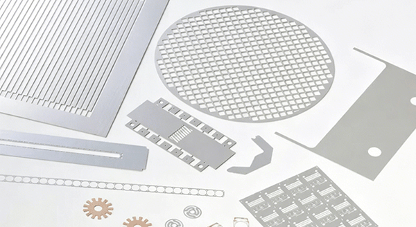
Ultra-Thin Copper Alloy Chemical Etching: Full Process Flow, Core Features & Industrial Applications
Ultra-thin copper alloys — including high-purity copper, beryllium copper, phosphor bronze and cupronickel, typically in gauges below 0.1mm — are critical functional materials in high-end micro-manufacturing. Their exceptional electrical conductivity, thermal conductivity, elastic resilience and corrosion resistance make them indispensable for semiconductor packaging, 5G communications, consumer electronics and medical devices. However, the extremely thin gauge presents major fabrication challenges: stamping easily causes foil tearing, edge curling and work hardening that degrade elastic and conductive performance; laser cutting creates heat-affected zones, thermal warping and recast layers that reduce signal integrity; mechanical punching suffers from severe burrs and high scrap rates. Chemical etching, a non-contact cold manufacturing technology, achieves high-precision patterning on ultra-thin copper alloys through photolithographic pattern transfer and controlled liquid-phase dissolution. It avoids all the above defects and fully retains native material properties, making it the mainstream processing solution for ultra-thin precision copper components.
I. Full Process Flow of Ultra-Thin Copper Alloy Chemical Etching
Designed for the high sensitivity of thin copper foils to oxidation, stress and thermal impact, the etching process follows a rigorously controlled, step-by-step production chain with tailored parameters for each alloy grade and thickness to ensure optimal precision and surface integrity.
1. Surface Pre-Treatment & Degreasing
Ultra-thin copper surfaces are highly prone to oxidation and residual oil stains, which directly reduce photoresist adhesion and cause uneven etching. This step includes ultrasonic degreasing to remove surface contaminants, mild pickling to eliminate thin oxide layers, and micro-roughening to create a uniform micro-textured surface for enhanced photoresist bonding. All operations use gentle process parameters to avoid foil deformation and excessive material loss.
2. Photoresist Coating & UV Exposure
A uniform, ultra-thin layer of UV-sensitive photoresist is applied to the pre-treated copper surface, with coating thickness precisely calibrated according to foil gauge and target etching depth. A high-resolution photomask carrying the target design is then aligned with the workpiece with micron-level accuracy, and controlled low-energy UV exposure polymerizes the photoresist in exposed areas to form a corrosion-resistant masking layer. For ultra-thin foils, reduced exposure energy prevents photoresist penetration and substrate damage.
3. Development & Low-Temperature Curing
After exposure, unpolymerized photoresist in unexposed areas is washed away by developer solution, transferring the target pattern accurately to the photoresist layer. Development time is tightly controlled to avoid undercut of the resist pattern. The workpiece then undergoes low-temperature thermal curing to strengthen photoresist adhesion and corrosion resistance, with temperature strictly limited to prevent thermal warping of the thin copper foil.
4. Precision Controlled Chemical Etching
The workpiece is fed into an automated spray etching chamber, where formulated copper etchant is uniformly sprayed onto both sides. By precisely controlling etchant concentration, temperature, spray pressure and conveyor speed, selective dissolution of exposed copper alloy is achieved. For ultra-thin foils, low-concentration etchant and gentle spray parameters are used to prevent over-etching and foil wrinkling, while side etching is strictly regulated to preserve pattern fidelity.
5. Photoresist Stripping & Anti-Oxidation Post-Treatment
Once etching reaches the target depth, the workpiece enters a stripping station to completely remove residual photoresist with mild stripping agents that do not attack the copper surface. It then undergoes multi-stage pure water cleaning, passivation treatment and low-temperature drying. The passivation step forms a dense protective film on the copper surface to prevent natural oxidation and discoloration during storage and use.
6. Quality Inspection & Clean Packaging
Finished parts undergo comprehensive inspection including dimensional tolerance verification, edge quality examination and surface condition assessment via high-precision optical measuring instruments. High-value components receive full visual inspection to eliminate defects. Final parts are packed in clean, anti-static and anti-oxidation packaging to prevent scratching and tarnishing during transit.
II. Core Technical Features of Ultra-Thin Copper Alloy Etching
The room-temperature liquid-phase reaction mechanism gives chemical etching unique advantages for ultra-thin copper alloy processing, directly addressing long-standing pain points of traditional fabrication methods.
1. Zero-Stress Cold Processing with No Thermal Damage
Operating entirely at ambient temperature with no mechanical punching force or high-temperature thermal input, the process eliminates foil tearing, warping and work hardening. The native electrical conductivity, thermal conductivity, elastic resilience and corrosion resistance of copper alloys are 100% preserved. This is particularly critical for beryllium copper elastic components and high-purity copper conductive parts, where even minor performance degradation can cause product failure.
2. Burr-Free Smooth Edges with No Secondary Finishing
Material is removed at the molecular level through uniform chemical dissolution, producing smooth, rounded edges completely free of burrs, flash and sharp protrusions. For high-frequency signal components, burr-free edges avoid signal reflection and tip discharge, ensuring stable transmission performance. For elastic parts, smooth profiles prevent stress concentration and extend fatigue life. Finished parts can proceed directly to assembly without secondary deburring, grinding or polishing.
3. Micron-Level Accuracy with Excellent Full-Sheet Uniformity
For ultra-thin copper foils, dimensional tolerance is stably controlled at ±0.005mm, with a minimum machinable line width of 0.015mm. Since all features form simultaneously through uniform chemical reaction, there is no cumulative positioning error, and dimensional consistency across the full workpiece exceeds 99.5%. Automated closed-loop production ensures stable accuracy from the first part to the ten-thousandth part, with no quality drift from tool wear.
4. Full Retention of Native Material Properties
The process does not alter the metallographic structure of copper alloys or damage the surface passive film. Electrical conductivity, elastic modulus and corrosion resistance remain identical to the raw material, unlike laser cutting which causes edge embrittlement and reduced corrosion resistance, or stamping which introduces work hardening and residual stress.
5. Precision Half-Etching for Integrated Micro-Features
Beyond full through-etching, chemical etching supports highly accurate half-etching for partial-depth surface features, with depth tolerance controlled within ±0.003mm. This enables integrated formation of bending positioning grooves, sealing recesses and step structures in a single process step, eliminating secondary machining and improving assembly alignment accuracy.
6. Tooling-Free Design Flexibility
No dedicated hard tooling is required, and there is no geometric complexity penalty. Complex curves, dense hole arrays, fine spring fingers and irregular custom contours all form in one process step at the same unit cost as simple shapes. Design modifications only require updating the photomask file with no additional mold costs, supporting rapid design iteration and customized production.
7. Stable Batch Consistency for Mass Production
Since there is no physical tool to wear out, dimensional accuracy and edge quality remain completely consistent across long production runs. This long-term batch stability meets strict quality traceability requirements for electronics and medical industries, reduces incoming inspection workload and supports large-scale volume production.
III. Core Functional Values & Industrial Significance
Beyond basic shape forming, ultra-thin copper alloy etching delivers six core functional values that solve long-standing manufacturing pain points and create tangible economic benefits for downstream industries.
1. High-Performance Conductive & Elastic Structure Forming
The most fundamental function is to fabricate high-precision conductive and elastic components while fully retaining copper alloy properties. From ultra-thin connector contacts to micro spring elements, etching ensures stable electrical conductivity and reliable elastic performance, providing core component support for electrical connection and signal transmission systems.
2. High-Density High-Frequency Signal Integrity Assurance
For high-speed communication and high-frequency scenarios, burr-free, damage-free etched copper structures ensure signal integrity, reduce transmission loss and avoid electromagnetic interference. This supports the continuous upgrading of electronic and communication products toward higher frequency, higher speed and higher density.
3. Miniaturized Integrated Device Enabling
Etching integrates multiple functional features such as contacts, mounting holes and positioning structures onto a single thin copper sheet in one step, replacing multi-part assembly solutions. This reduces product volume and weight, improves structural reliability and lowers total system cost, supporting the industry-wide trend of electronic product miniaturization.
4. Agile R&D and Rapid Prototyping
Low-cost photomask tooling enables prototype delivery within 24–48 hours, supporting rapid verification of different design, material and thickness options. There is no expensive mold investment, greatly reducing R&D trial-and-error costs and shortening product launch cycles.
5. Total Lifecycle Cost Optimization
Chemical etching eliminates expensive mold costs, reduces secondary finishing processes and achieves high production yield. For small and medium batch orders and customized high-performance copper components, total manufacturing cost is significantly lower than traditional processes. The long service life of stress-free, burr-free parts also reduces replacement and maintenance costs.
6. High-Cleanliness Compliance for Sensitive Industries
The burr-free, particle-free surface finish meets strict cleanliness requirements for semiconductor and medical applications. There are no loose metal particles that could cause clogging, short circuits or tissue damage during service. Etched parts are easy to clean and sterilize, complying with stringent industry hygiene and safety standards.
IV. Key Industrial Application Fields
Thanks to its unique advantages in ultra-thin copper processing, chemical etching serves a fast-growing range of high-tech and industrial sectors.
1. Semiconductor & Advanced Packaging
This is the largest and most core application field. Etched ultra-thin copper components include ultra-fine pitch lead frames, miniaturized EMI shielding cans, micro connector spring contacts and vapor chamber wick structures. High precision and full conductivity retention perfectly support the trend toward smaller, denser and more reliable semiconductor packaging.
2. Telecommunications & RF Devices
In 5G communications and radio frequency industries, etched copper alloy components include antenna elements, filter resonators, high-speed connector contacts and waveguide structures. Burr-free smooth edges ensure stable, low-loss high-frequency signal transmission, meeting the strict performance requirements of modern communication systems.
3. Consumer Electronics & Wearable Devices
Smartphones, wireless earbuds, smart watches and wearable devices incorporate a wide range of etched ultra-thin copper parts, such as speaker spring diaphragms, camera VCM springs, wireless charging coils and heat dissipation meshes. Ultra-thin forming capability and high precision perfectly match the consumer electronics industry’s demands for slim design, miniaturization and stable large-scale supply.
4. Medical Devices & Life Sciences
Medical-grade etched copper components include implantable electrode sheets, infusion filter meshes, biosensor elements and minimally invasive surgical instrument accessories. Burr-free smooth surfaces avoid tissue damage, and passivated surfaces meet biocompatibility requirements, supporting applications from surgical instruments to in-vitro diagnostic equipment.
5. Precision Instrumentation & Optoelectronics
Etched copper parts are used for optical slits, diaphragms, encoder gratings and precision relay contacts in spectrometers, laser systems and precision measuring instruments. Micron-level edge accuracy ensures excellent optical and sensing performance, providing reliable support for high-precision instrumentation.
6. New Energy & Energy Storage
Ultra-thin etched copper meshes serve as current collectors and electrode substrates for micro fuel cells and supercapacitors. Uniform pore distribution ensures consistent current density and reaction interface area, improving energy density and cycle life of energy storage devices, while the ultra-thin substrate supports lightweight system design.
7. Automotive Electronics
The automotive industry uses etched ultra-thin copper parts including vehicle sensor springs, connector contacts and battery system components. Stress-free processing ensures long-term reliable performance under harsh vehicle operating conditions such as vibration, temperature fluctuations and corrosive environments, meeting strict automotive-grade quality requirements.
Conclusion
In summary, ultra-thin copper alloy chemical etching breaks through the processing bottleneck of traditional technologies for thin-gauge high-performance copper materials, delivering a high-precision, low-damage and flexible manufacturing solution through a rigorously controlled production flow. With core advantages including zero stress, burr-free edges, full material property retention and tooling-free customization, it strongly supports performance upgrades across semiconductors, telecommunications, consumer electronics and medical industries, and has become an indispensable micro-fabrication technology for ultra-thin precision copper components.
As global products continue to advance toward miniaturization, high-frequency interconnection and higher reliability, market demand for ultra-thin high-precision copper alloy components will keep growing. Looking ahead, ultra-thin copper etching technology will evolve toward higher resolution, tighter process control and more environmentally friendly etchant systems, further expanding its application scope and providing stronger technical support for product innovation and industrial upgrading across more high-end manufacturing sectors.