
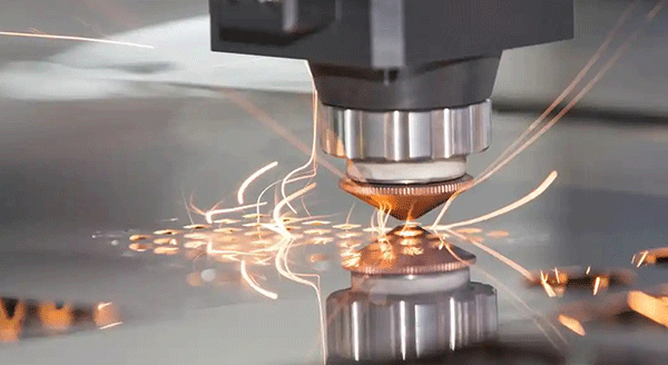
Ultra-Thin Copper Alloy Laser Cutting: Process Flow, Core Features & Industrial Applications
Ultra-thin copper alloys, including high-purity copper, beryllium copper, phosphor bronze and cupronickel typically under 0.1mm in thickness, are core functional materials in micro-electronic and precision manufacturing sectors. Their outstanding electrical conductivity, thermal conductivity and elastic resilience make them indispensable for semiconductor packaging, 5G communications, wearable electronics and medical devices. However, the extremely thin gauge and high reflectivity of copper create notable fabrication challenges: stamping easily causes foil tearing, edge curling and work hardening; chemical etching requires mask preparation and longer lead times; traditional CO₂ lasers suffer from high reflectivity and severe thermal damage. Modern pulsed fiber laser cutting, optimized for highly reflective materials, delivers non-contact, high-precision shaping on ultra-thin copper alloys with tightly controlled thermal impact and no tooling costs. It has become a mainstream processing solution for custom, small-batch and fast-turnaround ultra-thin copper components.
I. Complete Process Flow of Ultra-Thin Copper Alloy Laser Cutting
Designed for the high reflectivity, thin gauge and thermal sensitivity of copper alloys, the laser cutting process follows a rigorously controlled workflow with tailored parameters for each alloy grade and thickness to ensure optimal edge quality and minimal thermal deformation.
1. Material Preparation & Surface Pre-Treatment
Raw ultra-thin copper foils are first inspected for surface oxidation, oil stains and flatness defects. Light surface cleaning is performed to remove contaminants and residual protective films, ensuring consistent laser energy absorption during cutting. For foils thinner than 0.05mm, special flattening treatment is applied to eliminate wrinkles and warping, avoiding positioning errors and cutting discontinuities during processing.
2. Digital Programming & Optical Path Calibration
CAD design files are imported into the CNC laser control system, and cutting paths, sequence and process parameters are optimized according to part geometry and copper alloy properties. Before production, the laser optical path, focal length and assist gas pressure are calibrated to ensure consistent beam quality across the entire processing area. For highly reflective copper materials, anti-reflection optimized fiber lasers and beam shaping modules are used to improve energy absorption efficiency and reduce back-reflection damage to the resonator.
3. Precision Fixturing & Focal Positioning
Ultra-thin copper foils are fixed on a dedicated vacuum adsorption platform to ensure full flatness and avoid vibration or displacement during high-speed cutting. The laser focal point is precisely positioned at or slightly below the material surface to achieve the narrowest kerf and minimum heat-affected zone. For foils as thin as 0.01mm, defocus parameters are finely tuned to prevent direct penetration damage and edge over-burning.
4. Pulsed Laser Precision Cutting
High-frequency pulsed laser beams are used for cutting, with pulse width, peak power and cutting speed matched to material thickness and alloy type. Compressed air or nitrogen assist gas is blown coaxially with the beam to blow away molten copper material, cool the cutting edge and reduce oxidation. For ultra-thin foils, short-pulse, high-frequency parameters are adopted to minimize heat input, control the heat-affected zone within 10–20μm, and avoid warping, curling and performance degradation caused by heat accumulation.
5. Post-Processing & Anti-Oxidation Treatment
After cutting, parts undergo mild surface cleaning to remove a small amount of molten residue on the edge. For applications with high conductivity and corrosion resistance requirements, anti-tarnish passivation treatment is applied to form a thin protective film on the copper surface, preventing natural oxidation and discoloration during storage and use. For high-demand scenarios, light deburring or polishing can be added to further improve edge smoothness.
6. Quality Inspection & Clean Packaging
Finished parts are inspected for dimensional tolerance, edge quality, surface oxidation and flatness using high-precision optical measuring instruments. Critical components receive 100% visual inspection to eliminate defective products. Qualified parts are packed in anti-static, anti-oxidation and scratch-proof packaging, with protective interlayers to avoid deformation and damage during transportation.
II. Core Technical Features of Ultra-Thin Copper Alloy Laser Cutting
Optimized pulsed laser technology overcomes the traditional bottlenecks of copper processing, giving laser cutting unique technical advantages for ultra-thin copper alloy fabrication.
1. Ultra-Minimal Heat-Affected Zone & Low Deformation
With short-pulse fiber laser technology and optimized cooling assist gas, the heat-affected zone at the cutting edge is controlled within 10–20μm, far smaller than conventional laser cutting. For ultra-thin copper foils, thermal accumulation is effectively suppressed, avoiding obvious warping, curling and material property degradation. The non-contact processing mode applies no mechanical pressure, eliminating foil tearing and stress deformation common in stamping.
2. Micron-Level Dimensional Accuracy
Professional ultra-thin copper laser cutting achieves stable dimensional tolerance of ±0.008mm to ±0.015mm, with kerf width as narrow as 0.02mm. Supported by high-precision linear motor platforms and closed-loop feedback systems, positioning accuracy is consistent across the entire processing area with no edge accuracy attenuation. This level of precision meets the demanding dimensional requirements of micro-electronic and RF components.
3. Clean Burr-Free Edge Quality
With optimized laser energy distribution and assist gas parameters, cut edges are smooth and neat with almost no burrs, molten slag or hanging nodules. For most industrial applications, finished parts can enter assembly directly without heavy secondary deburring. Compared with punched and mechanically sheared foils that often leave sharp burrs, laser-cut parts avoid risks such as circuit shorting, signal interference and tissue scratching during service.
4. Tooling-Free Design Flexibility
Laser cutting requires no dedicated hard tooling. Complex contours, fine slits, irregular shapes and custom patterns are all processed directly from digital CAD files. Design modifications only require updating the electronic drawing with no additional mold cost or debugging lead time. This gives engineers complete freedom to optimize part geometry for electrical, thermal and mechanical performance, without manufacturing process constraints.
5. Wide Compatibility Across Copper Alloy Grades
The process works reliably with virtually all common copper alloy materials, including pure copper, brass, phosphor bronze, beryllium copper and cupronickel, with applicable thickness ranging from 0.01mm ultra-thin foil to 1mm thin plate. Targeted process parameters are configured for different reflectivity and thermal conductivity grades to ensure stable cutting quality. Even for high-hardness beryllium copper which is difficult to machine mechanically, laser cutting achieves clean, damage-free forming.
6. Stable Batch Consistency
The entire cutting process runs under fully automatic closed-loop control, with real-time monitoring and dynamic compensation of laser power, cutting speed and focal position. Since there is no physical tool wear, dimensional accuracy and edge quality remain consistent from the first workpiece to the ten-thousandth, with no gradual quality degradation over long production runs.
7. Integrated Multi-Process Capability
In addition to contour cutting, the same laser system can perform surface marking, micro-scoring and micro-hole drilling in a single clamping. This eliminates secondary positioning errors, improves overall processing accuracy and simplifies the production flow. For complex copper components with multiple functional features, integrated processing significantly shortens lead times and reduces total manufacturing costs.
III. Core Functional Values & Industrial Significance
Beyond basic shape forming, ultra-thin copper alloy laser cutting delivers six core functional values that solve long-standing manufacturing pain points and create tangible economic benefits for downstream industries.
1. Rapid Prototyping & Agile R&D Iteration
Thanks to tooling-free digital processing, prototype samples can be delivered within 24–48 hours after drawing confirmation, supporting fast verification of different design, material and thickness options. There is no expensive mold investment, greatly reducing R&D trial-and-error costs and shortening product launch cycles, which is especially valuable for fast-evolving electronics and communication sectors.
2. High-Precision Conductive & Elastic Structure Forming
Laser cutting produces fine conductive paths and elastic contact structures on ultra-thin copper alloys with minimal thermal impact on material properties. It preserves the vast majority of the base material’s native electrical conductivity and elastic resilience, providing core component support for high-density electrical connection and signal transmission systems.
3. Complex Miniaturized Part Fabrication
Laser cutting can fabricate extremely fine slits, micro-spring fingers and complex irregular contours that are difficult or impossible to achieve with stamping. This supports the continuing trend of product miniaturization and integration, enabling more compact, higher-performance electronic and medical devices.
4. Small-Batch Customization Flexibility
Laser cutting economically handles small and medium batch customized orders without absorbing mold costs. It can quickly respond to personalized requirements for different shapes, sizes and alloy grades, filling the market gap for high-precision custom ultra-thin copper components.
5. Total Manufacturing Cost Optimization
Although unit processing cost is slightly higher than high-volume stamping for very large orders, laser cutting eliminates expensive mold costs, reduces secondary finishing operations and achieves high yield for complex geometries. For small and medium batch orders and customized products, total manufacturing cost is significantly lower than traditional tooling-dependent processes.
6. Fast Lead Time & Supply Chain Responsiveness
Without mold preparation and long setup times, laser cutting achieves much shorter delivery cycles than stamping and chemical etching for custom orders. This helps downstream enterprises shorten supply lead times, respond faster to market demand changes and improve overall operational efficiency.
IV. Key Industrial Application Fields
Thanks to its unique combination of precision, flexibility and fast turnaround, ultra-thin copper alloy laser cutting serves a fast-growing range of high-tech and industrial sectors.
1. Semiconductor & Advanced Packaging
This is a core application field. Laser cutting is used to fabricate ultra-thin copper lead frames, micro shielding cans, connector contacts and heat spreader components. Its micron-level accuracy and minimal thermal impact perfectly match the high precision and high cleanliness requirements of semiconductor packaging.
2. Telecommunications & RF Devices
In 5G communication and radio frequency industries, laser-cut copper alloy components include antenna elements, filter resonators, high-speed connector contacts and waveguide structures. Clean, burr-free edges ensure stable low-loss high-frequency signal transmission, meeting the strict performance requirements of modern communication systems.
3. Consumer Electronics & Wearable Devices
Smartphones, wireless earbuds, smart watches and wearable devices use a large number of laser-cut ultra-thin copper parts, such as speaker spring diaphragms, camera VCM springs, wireless charging coils and heat dissipation meshes. Ultra-thin forming capability and high precision perfectly match the industry’s demands for slim design, miniaturization and stable mass supply.
4. Medical Devices & Life Sciences
Medical-grade laser-cut copper components include implantable electrode sheets, micro filter screens, biosensor elements and minimally invasive surgical instrument accessories. Smooth burr-free edges avoid tissue damage, and the process supports small-batch customized production of specialized medical components.
5. Precision Instrumentation & Optoelectronics
Laser-cut copper parts are used for optical slits, diaphragms, encoder gratings and precision relay contacts in spectrometers, laser systems and precision measuring instruments. Micron-level edge accuracy ensures excellent optical and sensing performance, providing reliable support for high-precision instrumentation.
6. New Energy & Energy Storage
Ultra-thin copper laser-cut meshes and current collector structures are used in micro fuel cells, supercapacitors and small battery systems. The fast, flexible processing capability supports R&D and small-batch production of new energy storage technologies.
7. Automotive Electronics
The automotive industry uses laser-cut ultra-thin copper parts including sensor springs, connector contacts and on-board electronic components. Stable batch consistency and reliable edge quality meet strict automotive-grade quality requirements for long-term performance under vibration and temperature fluctuation conditions.
Conclusion
In summary, ultra-thin copper alloy laser cutting breaks through the traditional processing bottleneck of highly reflective, thin-gauge copper materials, delivering a flexible, efficient and high-precision manufacturing solution through a rigorously controlled digital workflow. With core advantages including minimal heat-affected zone, micron-level accuracy, tooling-free design freedom and fast turnaround, it strongly supports performance upgrades across semiconductors, telecommunications, consumer electronics and medical industries, and has become an indispensable micro-fabrication technology for custom ultra-thin precision copper components.
As global products continue to advance toward miniaturization, high-frequency interconnection and faster R&D iteration, market demand for high-precision custom ultra-thin copper alloy components will keep growing. Looking ahead, ultrafast laser technology and more intelligent process control systems will further reduce thermal impact, improve cutting quality and expand application scenarios, providing stronger technical support for product innovation and industrial upgrading across more high-end manufacturing sectors.