
custom etched components
Photo etching, also known as photochemical machining (PCM), is a high-precision metal fabrication method widely used in the consumer electronics industry. It produces intricate, thin metal components without burrs or residual stress for smartphones, wearable devices, tablets, audio equipment, household appliances and other portable electronic products.
Consumer electronics features compact product structure, miniaturized internal parts and strict surface quality requirements. Even tiny burrs, deformation or metal particles may cause short circuits, assembly jams or cosmetic defects. Photo etching works by selectively removing metal through chemical corrosion after photoresist exposure. No hard tooling or strong mechanical force is applied, making it ideal for ultra-thin metal foils and complex micro patterns.
This process supports multiple common electronics-grade metals, including stainless steel, copper, nickel, brass and beryllium copper. The thickness range covers from 0.03mm thin foil to several millimeters, with micron-level dimensional tolerance to fit the limited inner space of compact consumer devices.
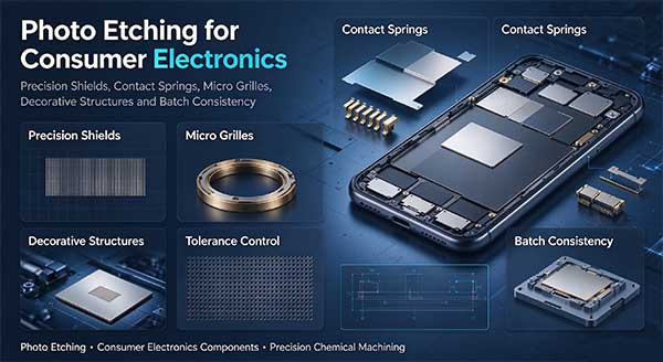
Typical Consumer Electronics Parts by Photo Etching
- EMI shielding sheets: Metal shielding frames for mobile phones, smart watches and Bluetooth earbuds
- Micro filter mesh: Speaker mesh, dust filter mesh for audio and wearable devices
- Spring contacts & conductive terminals: Etched spring tabs for battery and electrical connection
- Precision metal shims & washers: Thin spacers for gap adjustment in electronic assembly
- Decorative metal panels: Fine logo, pattern etched decorative sheets for consumer products
Core Advantages of Photo Etching in Consumer Electronics
- Burr-free and stress-free: No sharp edges to scratch flexible circuits or internal plastic parts
- High pattern flexibility: Complex cutouts, holes and logos can be modified quickly without expensive molds
- Ultra-thin material capability: Process ultra-thin foils that stamping cannot handle easily
- Consistent surface quality: Smooth surface meets electronics assembly and appearance requirements
- Fast prototyping: Short lead time for new product R&D, suitable for frequent design iterations
Stamping requires expensive custom molds and tends to deform thin metal workpieces. Laser cutting may leave thermal damage and rough edges on micro thin sheets. Photo etching avoids these drawbacks, ensuring stable part consistency during mass production. It greatly accelerates new product verification for consumer electronics brands.
We provide custom photo etching services for consumer electronics. Our engineers review customer CAD files, control tolerance strictly and carry out full inspection and cleaning before delivery for all etched electronic metal components.