
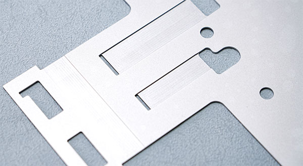
In the field of precision manufacturing, there is a special type of metal component: ultra-thin plates as thin as 0.01mm, intricate patterns and dense micro-holes, with extreme requirements on edge finish and dimensional consistency. Traditional stamping and ordinary laser cutting are faced with high mold costs and long R&D cycles. Moreover, they tend to cause thermal influence and mechanical stress, leading to part deformation and excessive burrs, which fail to meet high-end manufacturing standards. Precision chemical etching is the core technology to solve such processing problems, and it is the preferred solution for manufacturing ultra-thin metal parts.
Also known as photochemical etching, precision chemical etching forms metal parts through selective chemical corrosion. A protective mask is made on the metal surface, and special chemical solution dissolves the exposed metal areas to obtain parts with designed shapes. The whole process involves no mechanical force or high temperature, featuring zero stress, burr-free and anti-deformation performance. It is widely used in high-end industries such as electronic display, semiconductor, automotive electronics and medical devices. This article elaborates on its technical principles, core advantages, material adaptation and industry applications.
- Technical Principles and Complete Process of Precision Chemical Etching
1.1 Core Principle: Selective Chemical Corrosion
The core of precision chemical etching is selective dissolution. High-precision photolithography masks are produced according to product drawings to divide the metal substrate into different areas. The areas covered by masks are well protected, while the exposed areas are evenly corroded and removed by chemical liquid. The whole process relies purely on chemical reaction, with no tool contact, mechanical extrusion or high temperature. It fundamentally avoids stress deformation, burrs and slag, making it the ideal processing method for ultra-thin, miniature and complex-pattern metal parts.
1.2 Complete Technological Process
Drawing optimization and film production: Optimize drawings and produce high-precision exposure films to ensure pattern accuracy.
Substrate pre-treatment: Degrease, clean and dry metal plates to guarantee clean surface and enhance photoresist adhesion.
Glue coating and exposure: Coat photoresist evenly on plates and conduct ultraviolet exposure via films to cure photoresist on reserved areas.
Development and curing: Remove photoresist on unexposed areas with developer to expose etching zones, and strengthen mask layers by high-temperature curing.
Spray etching: Workpieces are sent to automatic etching equipment. Chemical solution is sprayed under high pressure for uniform corrosion to control depth and dimensions accurately.
Stripping and post-treatment: Remove residual photoresist, clean and dry products. Conduct polishing, passivation, electroplating and other surface treatments as required.
Inspection and packaging: Carry out full inspection on dimensions and appearance. Qualified products are vacuum packed to prevent oxidation and deformation.
- Core Advantages of Precision Chemical Etching
2.1 Zero stress, anti-deformation and burr-free
No mechanical force or high temperature is applied during processing. Ultra-thin metal plates will not be stretched, bent or warped. Part edges are naturally smooth without secondary polishing, which simplifies production procedures greatly.
2.2 Micron-level high precision and high consistency in mass production
Supported by photolithography technology, the machining tolerance reaches 卤0.01mm. The dimensions of micro-holes, dense lines and complex patterns are uniform and stable. Different from stamping, there is no dimensional deviation caused by mold wear, so the quality remains highly consistent in mass production.
2.3 One-time forming for complex patterns without molds
It can process ultra-complex planar structures such as dense micro-holes, special-shaped hollows and staggered lines in one step, with no need for customized stamping molds. It greatly reduces sampling costs, shortens delivery cycle, and adapts to products with multiple varieties, small batches and rapid iteration.
2.4 Wide material compatibility and full thickness coverage
It can process most common metals including stainless steel, copper, brass, aluminum, nickel, titanium and molybdenum, with processing thickness ranging from 0.01mm to 2mm. Stable etching effect can be achieved for both soft thin foils and high-hardness alloy plates.
2.5 Remarkable comprehensive cost advantages
No mold manufacturing cost leads to low upfront investment. Multiple parts can be etched on one plate simultaneously to reduce unit production cost. The mature and automatic process controls labor and time cost well, achieving high cost performance for both sampling and mass production.
- Characteristics and Processing Key Points of Mainstream Materials
3.1 Stainless Steel
With excellent corrosion resistance and stable mechanical properties, stainless steel is the most widely used material for etching. It is commonly made into metal meshes, electromagnetic shielding parts, precision gaskets and shrapnels, featuring neat edges and excellent overall performance after etching.
3.2 Copper and Brass
They have outstanding electrical and thermal conductivity, and are mostly used for conductive parts, heat dissipation components and RF shielding assemblies of electronic devices. Etching on ultra-thin copper foil will not damage its conductivity, so it is the mainstream choice for electronic circuit accessories.
3.3 Nickel and Nickel Alloy
Featuring high temperature resistance, corrosion resistance and good elasticity, nickel alloy is mainly used for battery poles, sensor parts and precision elastic components. The dimensions are accurate and elasticity will not be affected after etching.
3.4 Aluminum and Aluminum Alloy
Aluminum alloy is light and ductile, and easy to deform by traditional processing. Chemical etching realizes stress-free processing, which is widely used for ultra-thin lightweight parts of communication equipment and automobiles.
- Detailed Introduction of Industry Applications
4.1 Display and Semiconductor Industry
It is one of the core application fields of chemical etching. Fine Metal Masks (FMM) for OLED and Micro-LED screens adopt etching technology to process micron-level pixel micro-holes, ensuring clear images and uniform color. Precision parts such as semiconductor lead frames, wafer carriers and positioning fixtures also take etching as the core processing technology.
4.2 Electronics and Communication Industry
Various RF shielding covers, dust-proof metal meshes, conductive shrapnels and filter components are manufactured by chemical etching. Parts with complex hollow structures and dense micro-holes can be formed in one step to meet the demands of electromagnetic shielding, dust prevention and electrical conduction. It is widely applied to mobile phones, routers, base stations and other communication terminals.
4.3 Automotive and New Energy Industry
Etching is used to produce precision scales and holes for automotive electronic sensor grids and encoder discs. Ultra-thin current collectors and electrode plates for lithium batteries are formed by etching. It is also applied to precision structural parts of airbags and miniature automotive metal accessories. The stability and weather resistance of products meet strict vehicle standards.
4.4 Medical Device Industry
Medical industry sets strict standards on part cleanliness, biocompatibility and precision. Chemical etching can process miniature surgical parts, metal flow channels of microfluidic chips and precision accessories for diagnostic equipment made of titanium alloy and stainless steel. Its stress-free and pollution-free features fully comply with medical industry regulations.
- Key Points for Selecting Chemical Etching Suppliers
Enterprises shall evaluate suppliers from five aspects: First, equipment and production capacity. Give priority to manufacturers with fully automatic continuous etching production lines and high-precision image testing equipment to guarantee dimensional accuracy and production capacity. Second, material processing experience. Confirm that the supplier has rich experience in etching various metals and can optimize chemical liquid, temperature and spray parameters for different materials. Third, quality control system. Inspect quality inspection procedures, test reports and industry qualifications to ensure long-term stable product quality. Fourth, sampling and delivery capacity. Evaluate the efficiency of rapid sampling, mass production capacity and logistics delivery to match project progress. Fifth, industry service experience. Choose suppliers focusing on display, electronics, medical treatment, automobile and other fields, who are familiar with industry standards and customized requirements.
- Conclusion
Nowadays, electronic products are developing towards miniaturization, precision and ultra-thinness continuously, while the limitations of traditional processing technologies become increasingly obvious. The market value of precision chemical etching keeps rising. It perfectly solves the processing difficulties of ultra-thin metals, complex patterns and miniature parts, and has become an indispensable link in the high-end precision manufacturing industrial chain.
For enterprises requiring customized metal masks, etched meshes, ultra-thin conductive parts and precision shrapnels, cooperating with professional and reliable chemical etching suppliers can effectively reduce R&D costs, shorten product launch cycle and improve end-product quality. With the upgrading of high-end manufacturing industry, precision chemical etching technology will continue to iterate and play a core role in more high-tech fields.