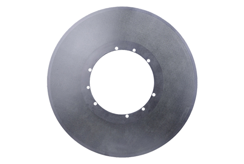
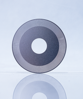
Material: SUS304
Thickness: 0.3mm
Precision Tolerance: ±0.01mm
Description:Semiconductor micro-probe laser processing features a small spot size, enabling the fabrication of 5-micron-level features with a tolerance of ±1 micron—significantly surpassing the ±5-micron tolerance achievable with traditional methods.

Why Laser Processing for Semiconductor Microprobes
Semiconductor microprobes are critical components in semiconductor testing, primarily used for wafer-level testing, chip functional verification, and defect detection. These micrometer-scale precision structures are typically made from tungsten, rhenium-tungsten alloys, or silicon-based materials, with diameters as small as tens of micrometers and lengths reaching hundreds of micrometers. These probes collect electrical signals by contacting chip pads, enabling high-density, multi-channel testing. As semiconductor processes advance toward the nanoscale and chip integration continues to increase, demands for probe precision, reliability, and consistency grow increasingly stringent. Traditional processing methods such as mechanical milling, electrochemical etching, or wire cutting present numerous limitations, failing to meet the demanding requirements of modern semiconductor testing. For instance, mechanical processing often produces burrs and deformation, while electrochemical methods involve chemical corrosion that can contaminate material surfaces.
Laser processing, as an advanced non-contact micro-machining technology, has become the mainstream choice for manufacturing semiconductor micro-probes. It utilizes high-energy-density laser beams for precise cutting, drilling, or surface modification, achieving sub-micron processing accuracy. The advantages of laser processing lie in its high precision, minimal thermal impact, and efficiency, significantly enhancing probe performance and yield. Industry data indicates that laser-processed microprobes achieve precision within ±1 micron, far surpassing the ±5 micron tolerance of traditional methods. This not only reduces testing errors but also extends probe lifespan, propelling the semiconductor industry toward higher integration levels. Driven by Moore's Law, laser processing has become a core technology for ensuring semiconductor test reliability. This article explores the reasons for adopting laser processing in semiconductor microprobes—covering principles, advantages, and applications—to reveal its technological value.
The core function of semiconductor microprobes is to bridge test equipment with chips, ensuring accurate signal transmission. Probe tips must be sharp and smooth to minimize contact resistance and damage risk. The introduction of laser processing enables more controllable and efficient fabrication of these microstructures. It supports both mass production and customized designs to accommodate diverse chip architectures.
Overview of Semiconductor Microprobes
Semiconductor microprobes are typically integrated into probe cards for functional testing of wafers in automated test equipment (ATE). Their complex structure comprises a probe body, tip, and mounting base. Tip diameters can reach as small as 20 micrometers, requiring flawless surfaces to prevent noise or short circuits during high-frequency testing. Material selection is critical: metal alloys offer excellent conductivity and mechanical strength, while silicon-based probes are compatible with MEMS processes.
Traditional manufacturing methods face significant challenges. Mechanical milling relies on tool contact, leading to probe bending or breakage, and its precision is limited by tool size, preventing sub-micron feature realization. Electrochemical etching can form intricate shapes but is slow, generates substantial chemical waste, and risks uneven material corrosion. Wire cutting is suitable for rough machining but creates large heat-affected zones and rough edges. These issues result in poor probe consistency, high scrap rates, and difficulty meeting testing demands for process nodes below 7nm.
The emergence of laser processing addresses these pain points. It is a material removal technique based on photothermal or photochemical effects, leveraging the spatiotemporal characteristics of lasers to achieve precision micro-machining. Common laser types include ultraviolet nanosecond lasers, picosecond lasers, and femtosecond lasers. Among these, picosecond lasers feature extremely short pulse durations (10^-12 seconds), minimizing thermal diffusion and making them suitable for brittle materials. Femtosecond lasers (10^-15 seconds) enable “cold processing” with virtually no heat-affected zone. These characteristics render lasers ideal for fabricating semiconductor microprobes, capable of creating complex geometries such as tapered tips or microgroove structures.
In probe manufacturing, lasers can be employed for cutting probe bodies, sharpening tips, or drilling mounting holes. Processing precision is high, achieving straightness up to 0.001mm/mm and surface roughness Ra < 0.1 micrometers. This is critical for enhancing probe contact performance, as rough surfaces increase resistance and compromise signal integrity. Additionally, laser processing supports high-density array fabrication, such as arranging thousands of probes within limited space, accommodating advanced packaging technologies like 3D stacked chips.
Principles of Laser Processing
The core principle of laser processing for semiconductor microprobes lies in the interaction between the laser and the material, involving photothermal effects, vaporization, melting, and plasma formation. The laser beam is focused by an optical system into a micrometer-scale spot (<5 micrometers), achieving energy densities as high as 10^9 W/cm². This rapidly heats the material to its vaporization point, enabling precise material removal.
The process occurs in several stages: First, laser absorption causes a rapid rise in material temperature; second, melting or vaporization forms the cut; finally, auxiliary gas (such as nitrogen) blows away residues to ensure a clean surface. For metal probes, infrared or green lasers are commonly used, with wavelengths of 1064 nm or 532 nm and power ranging from 10 to 50 W. In pulsed mode, the heat-affected zone is <10 micrometers, preventing material recrystallization or oxidation.
In silicon-based probe processing, ultraviolet lasers (355 nm) are more suitable due to their high photon energy, which can directly break molecular bonds to achieve non-thermal ablation. Femtosecond lasers are particularly well-suited for this purpose, featuring extremely short pulse widths that achieve edge perpendicularity >99% without microcracks. Typical workflow: Material fixed on precision stage → Import CAD design path → Laser scanning cut → Surface cleaning and inspection. Equipment integrates galvanometer systems and CCD vision feedback for closed-loop control, achieving positioning accuracy of ±0.5 microns.
Parameter optimization is critical: Excessive power causes thermal deformation, while low frequency reduces efficiency. By adjusting pulse energy and scanning speed, various feature sizes can be achieved. For instance, needle tip sharpening requires low power and slow scanning to ensure precise cone angles. Lasers can also be combined with other processes, such as surface modification to enhance wear resistance.
Overall, the principle of laser processing lies in its high selectivity and controllability, enabling micrometer-level operations without contacting the material. This is crucial for the intricate structures of semiconductor microprobes.
Advantages of Laser Processing
The primary reasons for adopting laser processing in semiconductor microprobes are its multiple significant advantages. First, high precision and resolution. The laser spot size is small, enabling the processing of 5-micron features with a tolerance of ±1 micron, far exceeding the ±5 micron tolerance of traditional methods. This ensures accurate probe array alignment and reduces testing deviations.
Second, non-contact processing avoids mechanical stress. Traditional methods risk probe deformation or fracture, whereas laser processing—being contactless—is ideal for brittle materials like silicon. The minimal heat-affected zone (<5 microns) prevents material property degradation, extending probe lifespan.
Third, efficiency and flexibility. Laser processing achieves speeds up to 1000 mm/s, supporting mass production. No molds are required, enabling direct CAD-driven operation and facilitating design iterations. Compared to the multi-step electrochemical etching process, laser processing simplifies to a single step, shortening production cycles.
Fourth, cleanliness and environmental friendliness. Lasers vaporize materials without generating chemical waste liquids, reducing pollution. Auxiliary gases ensure residue-free processing, making it suitable for cleanroom environments. Yield rates exceed 95%, lowering costs.
Fifth, multi-material compatibility. Lasers process metals, ceramics, and polymers, with adjustable parameters for varying hardness. High surface quality (Ra < 0.1 microns) enhances electrical contact performance.
Additionally, lasers support complex geometries like curved probes or microtextured surfaces, improving grip strength. Compared to other microfabrication methods, lasers offer greater reliability and repeatability, making them suitable for high-density probe cards.
Applications and Case Studies
Laser processing is widely adopted in semiconductor testing. For instance, in wafer testing, laser-cut microprobes enable high-frequency signal acquisition, ensuring accurate verification of nanoscale chips. In advanced packaging like fan-out wafer-level packaging (FOWLP), laser sharpening of probe tips enhances contact reliability.
Another application is MEMS probe fabrication. Laser drilling and patterning of silicon substrates form integrated probe arrays for biochip detection. Lasers also repair probes by precisely removing damaged layers to extend service life.
In high-power device testing, laser-processed metal probes withstand elevated temperatures, making them suitable for power semiconductors like IGBTs. Case studies demonstrate laser-fabricated probe arrays supporting tens of thousands of test channels, meeting AI chip demands.
Challenges and Advancements
Despite clear advantages, laser processing faces challenges such as energy loss in highly reflective materials and verticality control in thick materials. Solutions include employing short-wavelength lasers and multi-pass scanning. Future advancements with femtosecond lasers and AI optimization will push processing precision toward sub-micron levels. Integrating nanotechnology will further enhance probe performance.
Laser processing for semiconductor microprobes is favored for its high precision, non-contact nature, efficiency, and flexibility, driving semiconductor testing to new heights. This technology will play an increasingly vital role in the future semiconductor industry, fueling innovation.
Contact: Andy_Lai
Phone: +8613144801682
E-mail: info@lasercutoem.com
Add: 208, Building B, Fushengda, No. 6, Hongkan Road, Yanchuan Community, Yanluo Street, Bao'an District, Shenzhen, China